Infrared imaging detector based on carbon nano tubes and preparation method of detector

An infrared imaging and carbon nanotube technology, which is applied in nanotechnology, nanotechnology, nanotechnology and other directions for sensing, and can solve the problem of inability to meet the needs of weak light detection, low detector current responsivity, and small output photocurrent, etc. problem, to achieve the effect of improving current responsivity, reducing high cost, and reducing device resistance

Inactive Publication Date: 2014-03-26
PEKING UNIV
View PDF2 Cites 17 Cited by
  • Summary
  • Abstract
  • Description
  • Claims
  • Application Information

AI Technical Summary

Problems solved by technology

[0005] However, as far as the application of infrared photodetectors is concerned, an obvious shortcoming of the infrared detector based on a single carbon nanotube of this structure is that the output photocurrent is too small, and the current responsivity of the detector is low, which cannot meet the actual weak requirements. Light detection requires, mainly due to the relatively small light absorption area of ​​a single carbon nanotube material for incident light

Method used


Image

  • Infrared imaging detector based on carbon nano tubes and preparation method of detector
  • Infrared imaging detector based on carbon nano tubes and preparation method of detector
  • Infrared imaging detector based on carbon nano tubes and preparation method of detector

Examples


Embodiment Construction

[0040] The present invention will be further described below through specific embodiments and accompanying drawings.

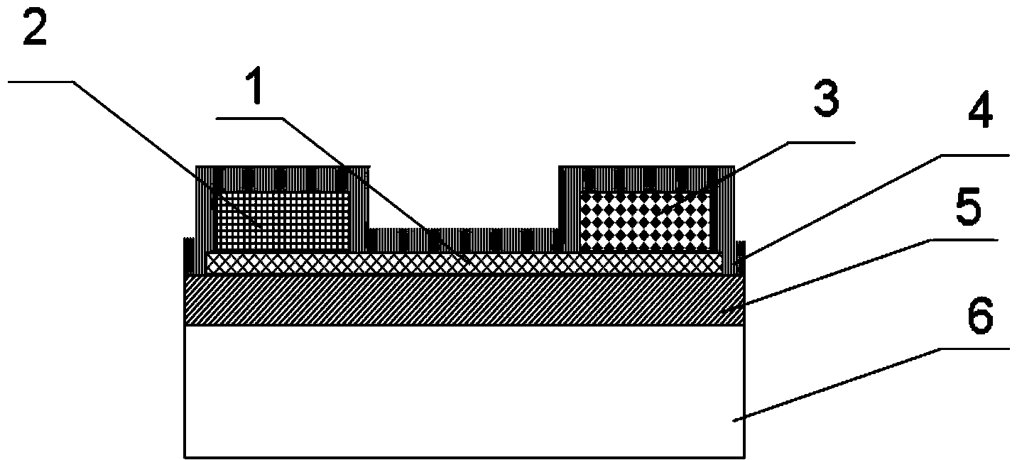
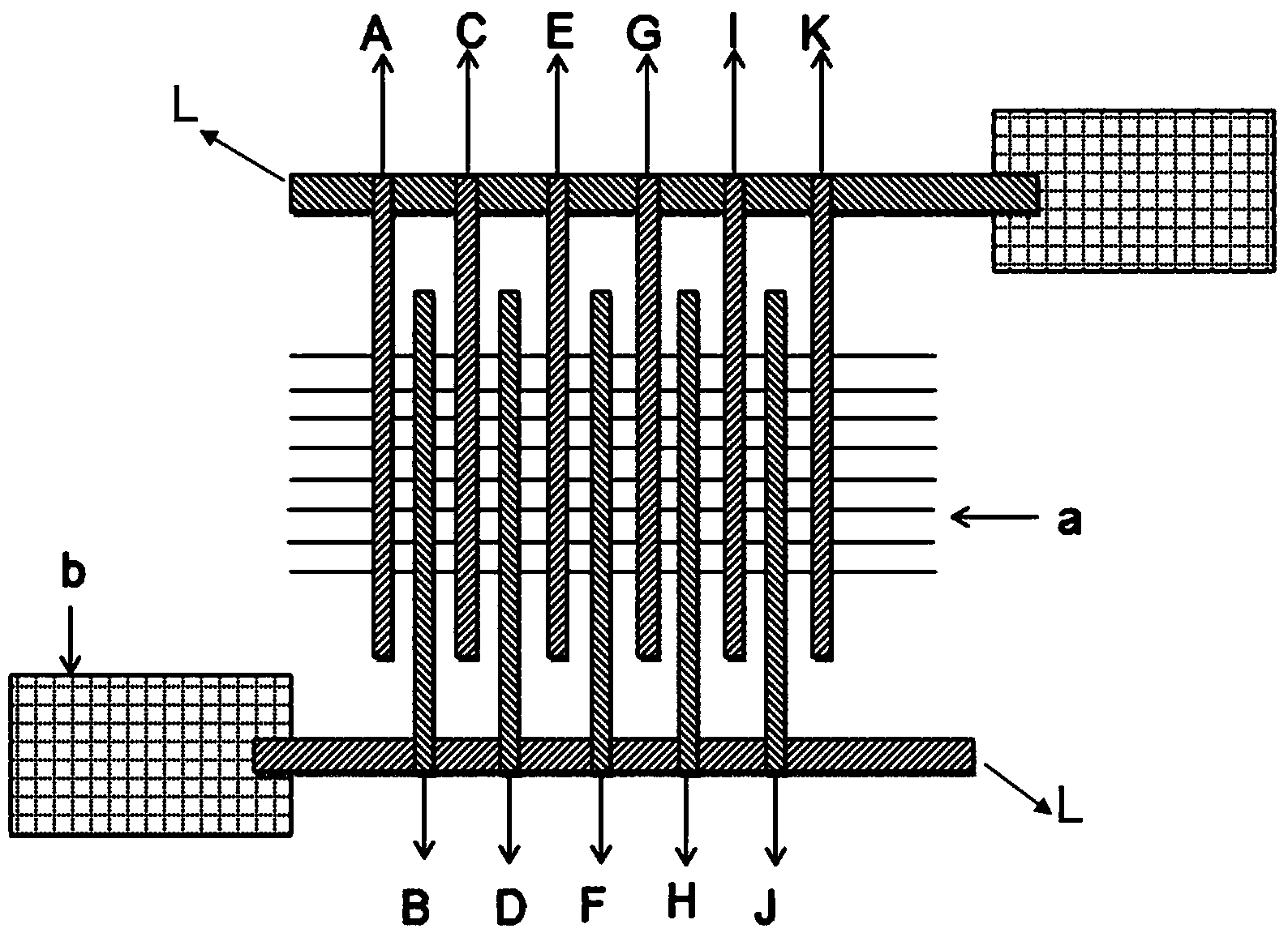
[0041] The infrared photodetector of the present invention can adopt several one-dimensional semiconducting carbon nanotubes, and can also adopt several semiconducting carbon nanotube film strips, which are similar in device preparation technology. image 3 It is the basic form of parallel infrared light detector using semiconducting carbon nanotube film strips. The width of the two asymmetric electrodes on the semiconducting carbon nanotube film strip is 0.5 micron, and the distance between the two asymmetric electrodes is 1 micron, wherein electrodes 1, 3, 5, 7, 9, and 11 are palladium Electrodes, electrodes 2, 4, 6, 8, and 10 are scandium (or yttrium) electrodes, and the specific process steps are as follows:

[0042] 1) Obtain the Si / SiO 2 Intrinsically high-density semiconducting carbon nanotube film strips a on substrate, using evaporation-driven self-...


PUM


Abstract

The invention discloses an infrared imaging detector based on carbon nano tubes and a preparation method of the detector. The infrared imaging detector comprises a substrate, a plurality of semiconductor carbon nano tubes or semiconductor carbon nano tube film strips located on the substrate, and asymmetrical contact electrodes. The asymmetrical contact electrodes include a plurality of first electrodes and a plurality of second electrodes. The first electrodes and the second electrodes are arranged at intervals and of ainterdigital electrode structure. The preparation method includes: using an evaporation drive self-assembling method to arrange the semiconductor carbon nano tubes or semiconductor carbon nano tube film strips on the substrate; forming the first electrodes, the second electrodes and the patterns of the metal connecting lines of the first electrodes and the second electrodes on the semiconductor carbon nano tubes or semiconductor carbon nano tube film strips, and evaporating the metal layers of the electrodes. The infrared imaging detector has the advantages that output photocurrent of the infrared detector is increased through parallel connection, device resistance is reduced, the device preparation process is simple, infrared detection can be achieve without doping, the output current is multiplied, and signal to noise ratio is increased.

Description

technical field [0001] The invention relates to an infrared photodetector, in particular to an infrared imaging photodetector prepared based on semiconductor carbon nanotubes, and a preparation method thereof. Background technique [0002] Infrared light detection is a very important direction in the field of light detection, and has been widely used in scientific fields, industrial and military applications, including monitoring, manufacturing process control, optical communication, biological and military night detection, etc. Infrared light detectors based on various materials are currently a research hotspot of scientists from all over the world. Infrared detectors based on traditional semiconductor materials, although they can achieve high quantum efficiency and good limit detection performance at low temperature, and can achieve high detection and fast response speed, but due to technical difficulties and complex processes, The price is high, and it is difficult to ap...

Claims


Application Information

Patent Timeline
Patent Type & Authority Applications(China)
IPC IPC(8): H01L31/0224H01L31/18H01L31/102B82Y15/00
CPCH01L31/022408H01L31/035227H01L31/102H01L31/18Y02P70/50
Inventor 王胜刘旸赵青靓魏楠张德辉彭练矛
Owner PEKING UNIV
Why Eureka
Try Eureka