

Emitter structure of crystal silicon heterojunction solar battery
A solar cell and emitter technology, applied in the field of solar cells, can solve the problems of increasing the recombination probability of photogenerated carriers, deteriorating the performance of solar cells, and increasing the density of defect states, so as to improve the open circuit voltage and filling factor, improve the photogenerated current and Efficiency, effect of low doping concentration
- Summary
- Abstract
- Description
- Claims
- Application Information
AI Technical Summary
Problems solved by technology
Method used
Image

Examples
Embodiment 1
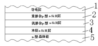
[0015] Embodiment 1: For a crystalline silicon battery using an n-type silicon wafer, a p-type layer is prepared to form a pn junction, and a specific implementation case is described in conjunction with the content of the present invention and in conjunction with the accompanying drawings, the present invention is further described.
[0016] The preparation sequence and performance parameters of the p-type double-layer gradiently doped emitter are as follows:
[0017] 1) Deposit a lightly doped a-Si:H layer on the prepared crystalline silicon wafer on which the intrinsic a-Si:H passivation layer has been deposited; the thickness of this layer is 15nm, and the doping concentration is 2×10 18 cm -3 . 2) Continue to deposit a heavily doped a-Si:H layer on the shallowly doped a-Si:H layer; the thickness of this layer is 3nm, and the doping concentration is 9×10 19 cm -3 .
[0018] After the gradient emitter is prepared, the TCO transparent conductive film, conductive grid lin...
Embodiment 2
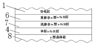
[0020] Example 2: For a crystalline silicon battery using a p-type silicon wafer, prepare an n-type layer to form a pn junction,
[0021] The preparation sequence and performance preparation of the n-type double-layer gradient doped emitter are as follows:
[0022] 1) Deposit a lightly doped a-Si:H layer on the prepared crystalline silicon wafer on which the intrinsic a-Si:H passivation layer has been deposited; the thickness of this layer is 15nm, and the doping concentration is 1.5×10 18 cm -3 . 2) Continue to deposit a heavily doped a-Si:H layer on the shallowly doped a-Si:H layer; the thickness of this layer is 3nm, and the doping concentration is 9×10 19 cm -3 .
[0023] After preparing the gradient emitter, install the same process as the emitter composed of a single-layer thin film to prepare TCO transparent conductive film, conductive grid lines and other structures.
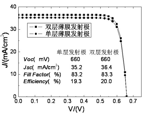
[0024] The obtained crystalline silicon heterojunction solar cell with a double-layer gradient d...
PUM
| Property | Measurement | Unit |
|---|---|---|
| Thickness | aaaaa | aaaaa |
| Thickness | aaaaa | aaaaa |
| Thickness | aaaaa | aaaaa |
Abstract
Description
Claims
Application Information