
Piezoelectric thin film, piezoelectric material, and fabrication method of piezoelectric thin film and piezoelectric material, and piezoelectric resonator

A manufacturing method and piezoelectric body technology, applied in the manufacture/assembly of piezoelectric/electrostrictive devices, piezoelectric devices/electrostrictive devices, piezoelectric/electrostrictive/magnetostrictive devices, etc., can solve Narrowing of the movable area, low piezoelectric constant, increased loss, etc., to achieve the effect of improving detection sensitivity, reducing insertion loss, and expanding the movable area

Active Publication Date: 2008-12-17
NAT INST OF ADVANCED IND SCI & TECH +1
View PDF1 Cites 25 Cited by
  • Summary
  • Abstract
  • Description
  • Claims
  • Application Information

AI Technical Summary

Problems solved by technology

That is, it is difficult to save power in devices using piezoelectric thin films having aluminum nitride, such as RF-MEMS devices.
[0012] In addition, since the piezoelectric constant is low, for example, when a piezoelectric thin film with aluminum nitride is used for an actuator, there will be problems as follows: Compared with an actuator made of a piezoelectric thin film made of a piezoelectric material with a high piezoelectric constant such as zinc oxide, the movable region is narrower, and when the piezoelectric thin film is used in a filter, the loss increases. question
That is, the low piezoelectric constant of aluminum nitride hinders the miniaturization and performance improvement of devices using piezoelectric thin films having aluminum nitride.

Method used


Image

  • Piezoelectric thin film, piezoelectric material, and fabrication method of piezoelectric thin film and piezoelectric material, and piezoelectric resonator
  • Piezoelectric thin film, piezoelectric material, and fabrication method of piezoelectric thin film and piezoelectric material, and piezoelectric resonator
  • Piezoelectric thin film, piezoelectric material, and fabrication method of piezoelectric thin film and piezoelectric material, and piezoelectric resonator

Examples


Embodiment approach 1

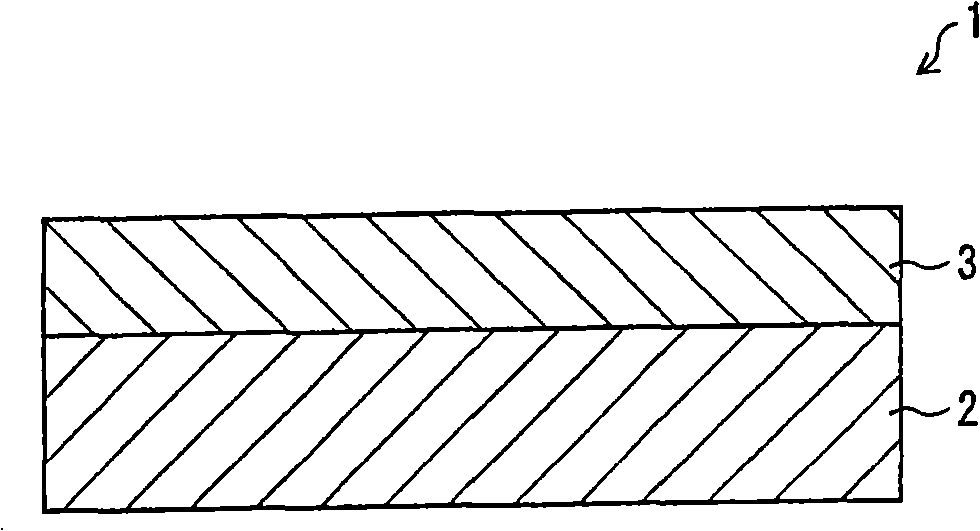
[0069] Refer below figure 1 and 2 , an embodiment of the piezoelectric thin film of the present invention will be described as Embodiment 1. FIG.

[0070] In addition, when the piezoelectric thin film of the present invention is used for a piezoelectric element utilizing a piezoelectric phenomenon, its specific use is not particularly limited. For example, piezoelectric thin films can be used in SAW devices or RF-MEMS devices. Here, a "piezoelectric body" in this specification and the like refers to a substance having piezoelectricity (hereinafter also referred to as piezoelectric responsiveness), which is a property of generating a potential difference when a mechanical force is applied. In addition, the term "piezoelectric thin film" refers to a thin film having the above properties.

[0071] In addition, the so-called "atomic %" in this specification etc. means an atomic percentage, specifically, it means the number of scandium atoms or the number of aluminum atoms when th...

Embodiment approach 2

[0088] Refer to the attached Figure 3-5 Another embodiment of the piezoelectric thin film of the present invention will be described as Embodiment 2. In this embodiment, the same components as in Embodiment 1 are given the same reference numerals. In addition, the same term as Embodiment 1 also uses the same meaning in this embodiment.

[0089] (Structure of Piezoelectric Thin Film 1b)

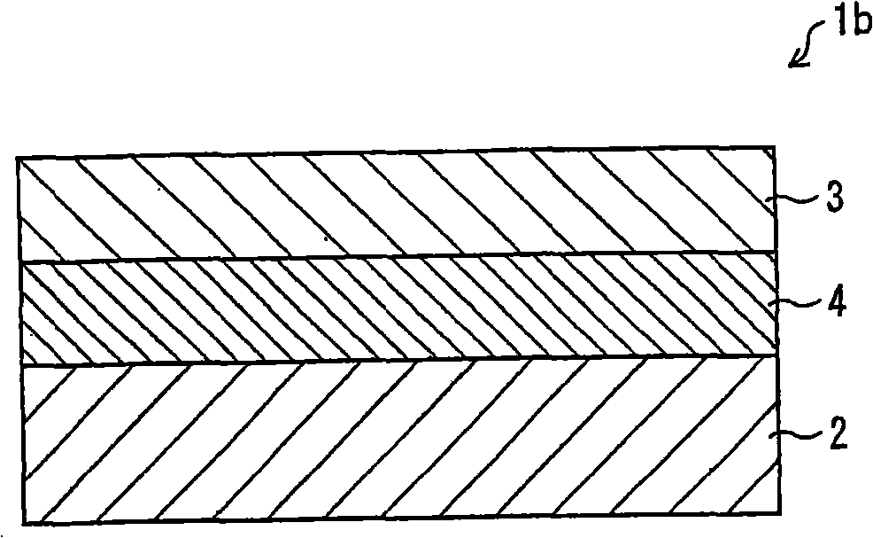
[0090] like image 3 As shown, in the piezoelectric thin film 1 b of the present embodiment, the intermediate layer 4 is formed between the substrate 2 and the Sc-containing aluminum nitride thin film 3 . That is, in the piezoelectric thin film 1b, the Sc-containing aluminum nitride thin film 3 is provided on the substrate 2 via the intermediate layer 4 . In the first embodiment, the substrate 2 and the Sc-containing aluminum nitride thin film 3 have been described, and thus detailed description thereof will be omitted here. Therefore, in this embodiment, only the intermediate layer 4 wi...

Embodiment approach 3

[0108] Refer below Image 6 One embodiment of the method for manufacturing the piezoelectric thin film 1 according to the first embodiment will be described as a third embodiment. In addition, the specific use of the Sc-containing aluminum nitride thin film is not particularly limited as long as it is used in a piezoelectric element utilizing the piezoelectric phenomenon. For example, a piezoelectric thin film having an Sc-containing aluminum nitride thin film can be used in a SAW device or an RF-MEMS device. In addition, in this embodiment, the same term as Embodiment 1 uses the same meaning.

[0109] The manufacturing method of the piezoelectric thin film 1 includes a sputtering process, that is, in nitrogen (N 2 ) atmosphere or nitrogen (N 2 ) and argon (Ar) in a mixed atmosphere, on the substrate 2 (for example, a silicon (Si) substrate) simultaneously sputtering scandium and aluminum. Thereby, the Sc-containing aluminum nitride thin film 3 having excellent adhesion an...


PUM

PropertyMeasurementUnit
Thicknessaaaaaaaaaa
Surface roughnessaaaaaaaaaa

Abstract

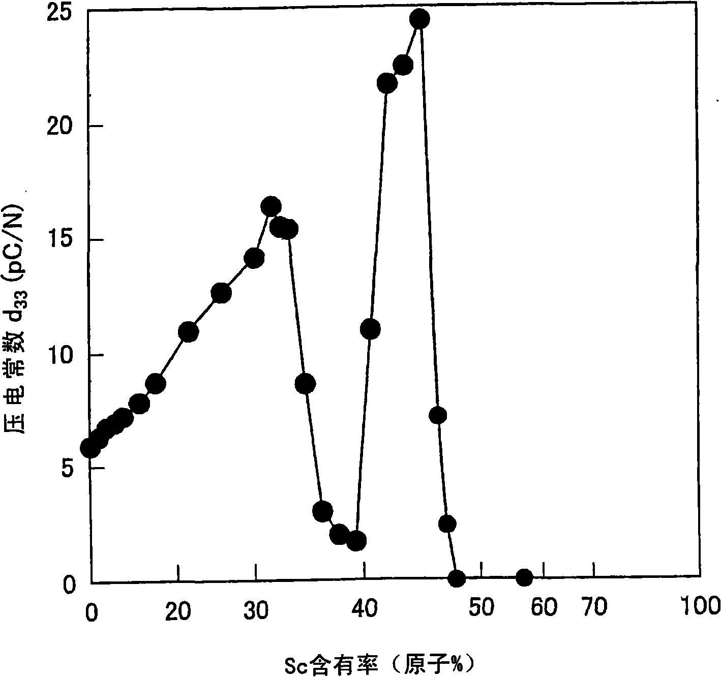
The invention relates to a piezoelectric thin film, a piezoelectrics and manufacturing method thereof, a piezoelectrics harmonic oscillator, a actuator element and a phsical sensor. A piezoelectric thin film of the present invention includes an aluminum nitride thin film that contains scandium. A content ratio of scandium in the aluminum nitride thin film is 0.5 atom % to 50 atom % on the assumption that a total amount of the number of scandium atoms and the number of aluminum atoms is 100 atom %. According to this arrangement, the piezoelectric thin film of the present invention can improve a piezoelectric response while keeping characteristics of elastic wave propagation speed, Q value, and frequency-temperature coefficient that the aluminum nitride thin film has.

Description

technical field [0001] The present invention relates to a piezoelectric body and a piezoelectric body film, in particular to a piezoelectric body in which scandium is added to aluminum nitride and a piezoelectric body film in which scandium is added to an aluminum nitride film. Background technique [0002] Devices utilizing the piezoelectric phenomenon are used in a wide range of fields, and their use is expanding in portable devices such as mobile phones that strongly demand miniaturization and power saving. As one example thereof, filters for IF (Intermediate Frequency: Intermediate Frequency) and RF (Radio Frequency: Radio Frequency) can be mentioned. Specific examples of filters for IF and RF include SAW filters, which are filters using surface acoustic wave resonators (Surface Acoustic Wave Resonators; SAWR). [0003] The SAW filter is a filter that uses a harmonic oscillator that utilizes sound waves propagating along the solid surface. Through the improvement of des...

Claims


Application Information

Patent Timeline
IPC IPC(8): H01L41/18H01L41/08H01L41/22H03H9/17H03H9/54H01L41/187H01L41/316H01L41/39H03H3/02H03H9/56
CPCH10N30/2047
Inventor 秋山守人蒲原敏浩上野直广加纳一彦勅使河原明彦竹内幸裕川原伸章
Owner NAT INST OF ADVANCED IND SCI & TECH
Learn More