Cell separation microchip based on silicon structure on insulators

A silicon-on-insulator, microchip technology, applied in the field of microchips for cell screening and separation, can solve the problems of weak electric field strength and electric field gradient, weak anti-corrosion, weak anti-oxidation ability, affecting the biological activity of cells, etc., so as to reduce physical damage. , low cost, mature processing technology

Inactive Publication Date: 2009-01-14
CHONGQING UNIV
View PDF2 Cites 24 Cited by
  • Summary
  • Abstract
  • Description
  • Claims
  • Application Information

AI Technical Summary

Problems solved by technology

[0006] At present, there is little research and development of cell separation chips in China. On the one hand, it is difficult for the existing cell separation chips to detect without adding any dyes or fluorescent materials (these will damage the cells and affect the biological activity of the cells); On the other hand, the

Method used


Image

  • Cell separation microchip based on silicon structure on insulators
  • Cell separation microchip based on silicon structure on insulators
  • Cell separation microchip based on silicon structure on insulators

Examples


Embodiment 1

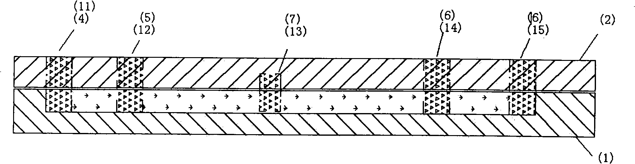
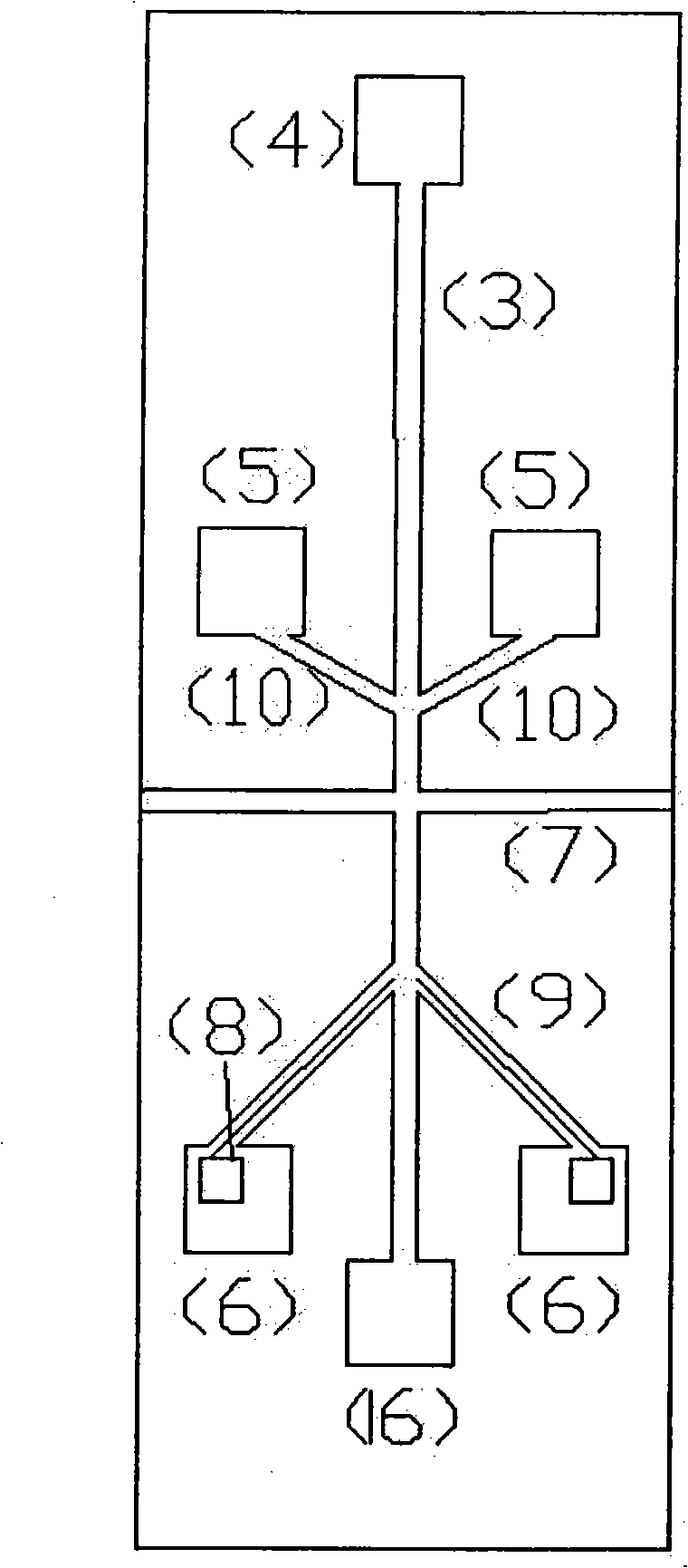
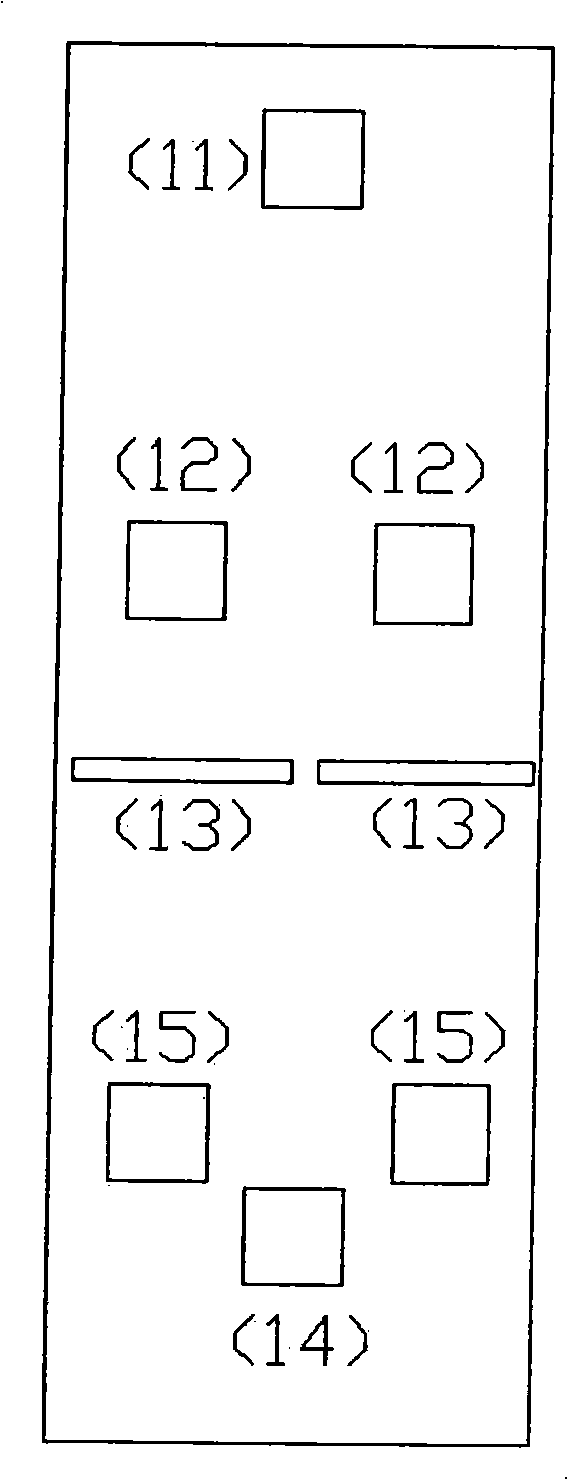
[0043] see figure 1 , 2 and 3, the microchip is composed of two layers bonded to each other, layer I is the channel layer 1, and layer II is the cover layer 2. The channel layer is a microstructure formed by etching grooves on the SOI silicon wafer using MEMS processing technology. The channel layer 1 has a main microchannel 3, a microchannel 9 connecting the main microchannel and the fusion cell pool, a sheath fluid channel 10, and a sample Pool 4, sheath flow pool 5, waste liquid pool 16, fusion cell pool 6, optical fiber groove 7 and microelectrode pair 8 structures, the sample pool 4 on the channel layer 1 is used for the storage of the sample liquid before screening; the main microchannel 3. The microchannel 9 and the sheath fluid channel 10 are kept unblocked for sample (cell suspension or solution) flow, and the optical fiber located in the optical fiber groove 7 provides an optical detection path; the microelectrode pair 8 realizes cell screening. The cover layer 2 i...


PUM


Abstract

The invention provides a cell separation microchip based on a silicon structure on an insulator, which consists of two mutually combined layers, wherein, the first layer adopts a path layer, and the second layer adopts a cover plate layer. A micro-structure is formed on the path layer through engraving grooves on an SOI silicon chip, the path layer is provided with a micro channel, a liquid storage tank, an optical fiber groove and a microelectrode couple structure, and the liquid storage tank on the path layer is used for sieving the former and the later sample liquids and storing sheath flow liquid; the micro channel is unimpeded and used for sample (cell suspension or solution) flow; optical fibers provide an optical detecting circuit; the microelectrode couple is used for realizing cell sieving. A sample inlet and a sample outlet on the cover plate layer are connected with an external pipe. The information of the cell volume can be obtained by the optical fibers for distinguishingwhether the cell is a fused cell or not, alternating current photo-electric signals are applied on the micro electrode couple correspondingly to deflect the cells, so the cell separation is realized. The chip utilizes an electric field to implement the non-contact sieving and separating operations to the biological live cells, so the survival rate of live cells is enhanced, the structure is simple, the process is convenient, and the cost is low.

Description

technical field [0001] The invention relates to a microchip for cell screening and separation, in particular to a cell separation microchip based on a silicon-on-insulator (SOI) structure. Background technique [0002] Biological cells can form new cells through fusion, which is of great significance in the basic field of modern biomedical engineering. Screening and separation of fused cells is a prerequisite for further culturing of fused cells, and effective screening and separation of fused samples is of great significance for cell fusion. At present, there are many methods that can realize cell screening and separation, such as fluorescence separation, DC electric field deflection, optical clamp, micromanipulation and so on. These methods usually require complex structures or delicate operations, are quite difficult to implement, cause great damage to cells, have poor experimental results, and are difficult to promote. [0003] When two homologous cells fuse, the volum...

Claims


Application Information

Patent Timeline
IPC IPC(8): C12Q1/04C12M1/42
CPCC12M47/04
Inventor 杨军杨静许蓉侯文生郑小林阴正勤胡宁廖彦剑
Owner CHONGQING UNIV
Why Eureka
Try Eureka