Solar cell and method of manufacturing the same

A technology of solar cells and electrodes, applied in circuits, photovoltaic power generation, electrical components, etc.

Inactive Publication Date: 2009-01-14
SAMSUNG SDI CO LTD
View PDF0 Cites 3 Cited by
  • Summary
  • Abstract
  • Description
  • Claims
  • Application Information

AI Technical Summary

Problems solved by technology

However, the passivation effect of the silicon nitride layer surface is less than that of the thermal oxide layer

Method used


Image

  • Solar cell and method of manufacturing the same
  • Solar cell and method of manufacturing the same

Examples


example 1

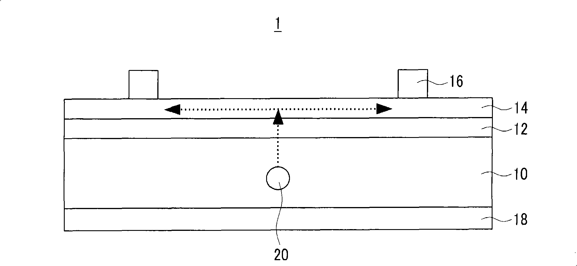
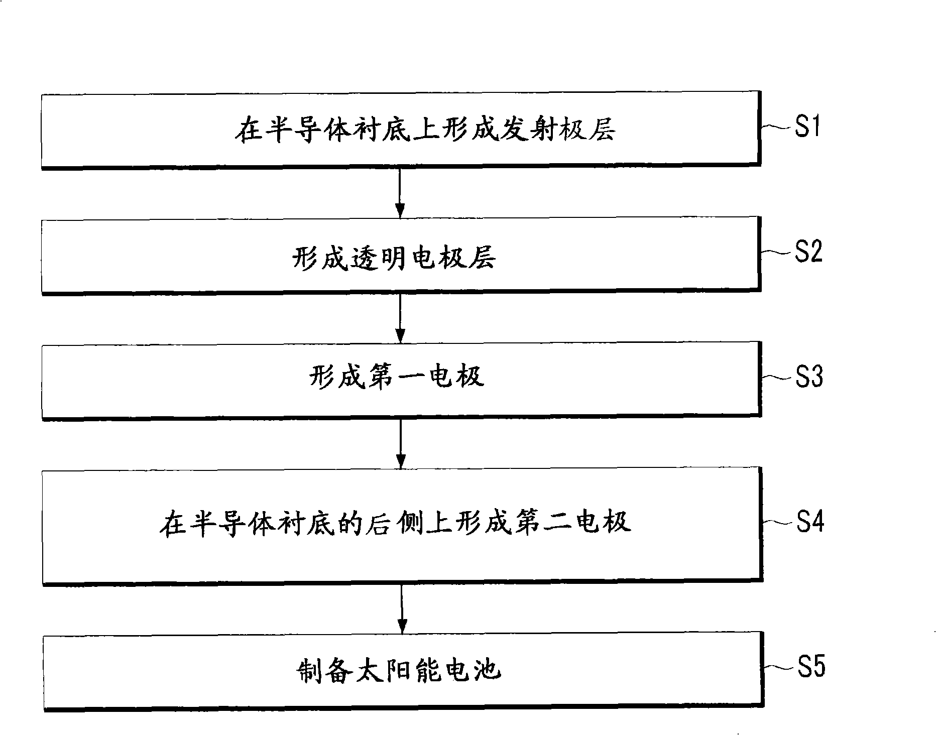
[0094] On one side of a boron-doped p-type silicon substrate (resistivity: 1Ω·cm), a 0.45 μm-thick emitter layer having phosphorous-doped n-type silicon was arranged. Boron at 1.5 x 10 16 / cm 3 amount doped into the p-type silicon substrate. The surface resistance of the emitter layer including n-type silicon was 50Ω per square.

[0095] Then, a conductive transparent electrode layer with a thickness of 80 nm was arranged on the emitter layer by sputtering.

[0096] An Al-containing paste was screen printed onto the other side of the p-type silicon substrate (ie, the side without the emitter layer). In addition, a p-type silicon substrate with a conductive transparent electrode layer was screen-printed with Ag-containing paste every 6 mm to form a pattern, and then sintered at 400 °C for 30 seconds to simultaneously (or parallel) form the first and second electrode, and then prepare a solar cell.

[0097] The emitter layer at the corners of the solar cell is laser removed...

example 2

[0099] On one side of a boron-doped p-type silicon substrate (resistivity: 1Ω·cm), a 0.3 μm-thick emitter layer with phosphorus-doped n-type silicon was arranged. Here, boron in 1.5×10 16 / cm 3 The amount is doped on the p-type silicon substrate. The surface resistance of the emitter layer including n-type silicon was 100Ω per square.

[0100] Then, on this emitter layer, an 80 nm-thick conductive transparent electrode layer was arranged using indium tin oxide (ITO) by a sputtering method.

[0101] Next, an Al-containing paste was screen printed on the other side of the p-type silicon substrate (ie, the side without the emitter layer). In addition, the p-type silicon substrate with the conductive transparent electrode layer was screen-printed with Ag-containing paste every 2.5 mm to form a pattern, and then fired at 400° C. for 30 seconds to simultaneously (or in parallel) ) to form the first and second electrodes, and then prepare a solar cell.

[0102] The emitter layer...

example 3

[0104] On one side of a boron-doped p-type silicon substrate (resistivity: 1Ω·cm), a phosphorous-doped n-type silicon emitter layer of 0.3 μm thick was arranged. Here, boron in 1.5×10 16 / cm 3 The amount is doped on the p-type silicon substrate. The surface resistance of the emitter layer including n-type silicon was 100Ω per square.

[0105] Then, on this emitter layer, an 80 nm-thick conductive transparent electrode layer was arranged using indium tin oxide (ITO) by a sputtering method.

[0106] An Al-containing paste was screen printed on the other side of the p-type silicon substrate (ie, the side without the emitter layer). In addition, the p-type silicon substrate with the conductive transparent electrode layer was screen-printed with Ag-containing paste every 6 mm to form a pattern, and then fired at 400° C. for 30 seconds to simultaneously (or in parallel) The first and second electrodes are formed to finally produce a solar cell.

[0107] The emitter layer at the...


PUM


Abstract

A solar cell having a high photoelectric efficiency by minimizing (or reducing) electron transfer resistance and electrode shading loss. The solar cell includes a semiconductor substrate; an emitter layer on a first side of the semiconductor substrate; a conductive transparent electrode layer on the emitter layer; a first electrode on the conductive transparent electrode layer and electrically connected to the conductive transparent electrode layer; and a second electrode on a second side of the semiconductor substrate and electrically connected to the semiconductor substrate. The conductive transparent electrode layer has a specific resistance of about 500[mu] CR m or less. The emitter layer may be doped with a low concentration of impurities resulting in improve optical response at a short wavelength and minimization (or reduction) of recombination loss.

Description

technical field [0001] The invention relates to a solar cell and a preparation method thereof. Background technique [0002] A solar cell generates electricity when electrons move to an n-type semiconductor while holes move to a p-type semiconductor due to an electric field generated by a p-n junction. Electrons and holes are generated inside the semiconductor due to energy provided by external light. [0003] Solar cells can be made as crystalline silicon solar cells, which include thin single crystals, polycrystalline and polycrystalline films. However, this type of solar cell has a problem in that defects on the surface and inside of silicon act as recombination centers for electron and hole pairs generated by external light, resulting in poor photoelectric efficiency. [0004] Defects in silicon can be passivated by forming a thermal oxide layer on its surface. Here too, the thermal oxide layer can function as an antireflection coating. Thus, various antireflection f...

Claims


Application Information

Patent Timeline
Patent Type & Authority Applications(China)
IPC IPC(8): H01L31/042H01L31/0224H01L31/18
CPCH01L31/1884H01L31/022466Y02E10/52Y02E10/50H01L31/0224H01L31/04H01L31/06H01L31/18
Inventor 文仁植金大园
Owner SAMSUNG SDI CO LTD
Why Eureka
Try Eureka