Nano CMOS integrated circuit preparation method based on SiN/SiO2 masking technique

An integrated circuit, nano-scale technology, applied in circuits, semiconductor/solid-state device manufacturing, electrical components, etc., can solve the problems of restricting the development of the semiconductor industry, waste of resources and energy, etc., to achieve leapfrog development, small conductive channels, The effect of increased manufacturing capacity

Inactive Publication Date: 2010-06-02
XIDIAN UNIV
View PDF4 Cites 0 Cited by
  • Summary
  • Abstract
  • Description
  • Claims
  • Application Information

AI Technical Summary

Problems solved by technology

This will lead to a huge waste of resources and energy. Therefore, this status quo seriously restricts the development of the semiconductor industry.

Method used


Image

  • Nano CMOS integrated circuit preparation method based on SiN/SiO2 masking technique
  • Nano CMOS integrated circuit preparation method based on SiN/SiO2 masking technique
  • Nano CMOS integrated circuit preparation method based on SiN/SiO2 masking technique

Examples


Embodiment 1

[0030] Embodiment 1: prepare the CMOS integrated circuit that conduction channel is 75nm on Si substrate, concrete steps are as follows:

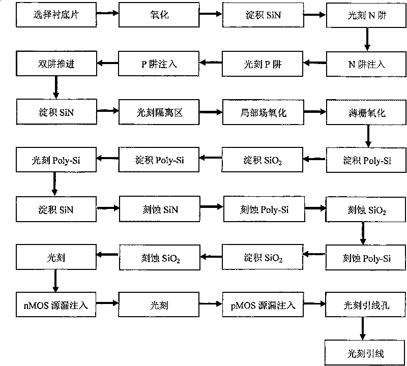
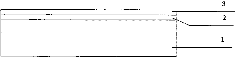
[0031] Step 1, deposit a masking layer, such as figure 2 (a) shown.

[0032] (1a) Select the crystal orientation as and the doping concentration as 10 15 cm -3 Left and right p-type Si substrate sheets 1;

[0033] (1b) Thermally oxidize a layer of SiO with a thickness of 20 nm on the substrate 2 buffer layer 2;

[0034] (1c) on SiO 2 A SiN layer 3 with a thickness of 80nm is deposited on the buffer layer by plasma enhanced chemical vapor deposition (PECVD), which is used for the masking of well implantation.

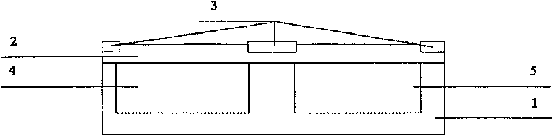
[0035] Step 2, forming a well region, such as figure 2 (b) shown.

[0036] (2a) Photoetching the P well region 4 and the N well region 5 on the SiN layer 3 according to the phase sequence;

[0037] (2b) Boron is implanted in the P well region to form a p-type region, and SiO is thermally oxidized on the surface of the P we...

Embodiment 2

[0066] Embodiment 2: prepare the CMOS integrated circuit that conduction channel is 65nm on SOI substrate, concrete steps are as follows:

[0067] Step 1, deposit a masking layer, such as figure 2 (a) shown.

[0068] (1a) Select the crystal orientation as and the doping concentration as 10 15 cm -3 left and right p-type SOI substrates 1;

[0069] (1b) Thermally oxidize a layer of SiO with a thickness of 30 nm on the substrate 2 buffer layer 2;

[0070] (1c) on SiO 2 A 100nm-thick SiN layer 3 is deposited on the buffer layer by atmospheric pressure chemical vapor deposition (APCVD) for the masking of well implantation.

[0071] Step 2, forming a well region, such as figure 2 (b) shown.

[0072] (2a) Photoetching the P well region 4 and the N well region 5 on the SiN layer 3 according to the phase sequence;

[0073] (2b) Boron is implanted in the P well region to form a p-type region, and SiO is thermally oxidized on the surface of the P well region 2 , while advanc...

Embodiment 3

[0102] Embodiment 3: prepare the CMOS integrated circuit that conduction channel is 90nm on Si substrate, concrete steps are as follows:

[0103] Step 1, deposit a masking layer, such as figure 2 (a) shown.

[0104] (1a) Select the crystal orientation as and the doping concentration as 10 15 cm -3 Left and right p-type Si substrate sheets 1;

[0105] (1b) Thermally oxidize a layer of SiO with a thickness of 40 nm on the substrate 2 buffer layer 2;

[0106] (1c) on SiO 2 A 120nm-thick SiN layer 3 is deposited on the buffer layer by low-pressure chemical vapor deposition LPCVD method, which is used for the masking of well implantation.

[0107] Step 2, forming a well region, such as figure 2 (b) shown.

[0108] (2a) Photoetching the P well region 4 and the N well region 5 on the SiN layer 3 according to the phase sequence;

[0109] (2b) Boron is implanted in the P well region to form a p-type region, and SiO is thermally oxidized on the surface of the P well region ...


PUM


Abstract

The invention discloses a method based on SiN / SiO2 masking technique for fabricating a nano-scale CMOS integrated circuit. The process includes the following steps: fabricating an N / P well and growinga Poly- Si / SiO2 / Poly-Si multi-layer structure on the N / P well; etching the top layer of Poly-Si into a window and then depositing a layer of SiN; etching the SiN layer on the surface, except the SiNat the side face of the window; based on the etching ratio of Poly-Si to SiN (11:1), etching the Poly-Si at the surface of SiN; based on the etching ratio of (4:1), etching the SiN on the surface, except the SiN on the side wall of SiO2; based on the etching ratio of Poly-Si to SiN, etching the Poly- Si, except the Poly- Si on the side wall of the SiO2 so as to form an n / p MOSFET grid; injecting ions, self-aligning, and forming the source area and the drain area of the n / p MOSFET grid so as to form an n / p MOSFET device; and photoetching interconnection lines of the device so as to form a CMOSintegrated circuit with a conducting channel at 65-90nanometer. The method can fabricate a CMOS integrated circuit which is improved in performance by 3-5 generations on a micron-scale Si integrated circuit processing platform without adding any funds and equipment investment.

Description

technical field [0001] The invention belongs to the technical field of semiconductor integrated circuits, and in particular relates to a method for manufacturing nanoscale CMOS integrated circuits by using the existing micron-scale Si integrated circuit manufacturing process. Background technique [0002] Today, information technology has become the core technology of the national economy. It serves all fields of the national economy. Microelectronics technology is the key to information technology, and integrated circuits are the key among the keys. Since the advent of integrated circuits in 1958, they have developed at an astonishing speed. They have become the core of information science and technology, the cornerstone of national economic development and national defense construction, and have had a huge impact on world politics, economy and culture. As the fastest-growing, most influential, and most widely used technology in human history, integrated circuits have becom...

Claims


Application Information

Patent Timeline
Patent Type & Authority Patents(China)
IPC IPC(8): H01L21/8238
Inventor 胡辉勇张鹤鸣戴显英宋建军舒斌宣荣喜赵丽霞王晓燕秦珊珊
Owner XIDIAN UNIV
Why Eureka
Try Eureka