Continuous flow cell electric amalgamation chip based on silicon structure on insulator

A silicon-on-insulator, electrofusion technology is applied in the field of biological cell electrofusion devices, which can solve the problems of corrosion resistance, anti-oxidation ability, weak precise control of cells, easy to be corroded, etc., so as to improve the efficiency of cell fusion, The effect of improving biocompatibility and improving electrical performance

Inactive Publication Date: 2009-02-18
CHONGQING UNIV
View PDF3 Cites 6 Cited by
  • Summary
  • Abstract
  • Description
  • Claims
  • Application Information

AI Technical Summary

Problems solved by technology

However, the number of integrated microelectrodes in the above patents is small, and high-throughput fusion cannot be achieved. On the other hand, the electric field strength and electric field gradient generated by the microelectrodes are relatively weak, which is relatively weak in terms of precise control of cells.
Chinese patent 200610054121

Method used


Image

  • Continuous flow cell electric amalgamation chip based on silicon structure on insulator
  • Continuous flow cell electric amalgamation chip based on silicon structure on insulator
  • Continuous flow cell electric amalgamation chip based on silicon structure on insulator

Examples


Embodiment Construction

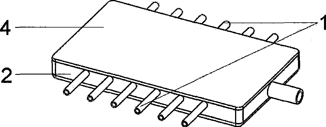
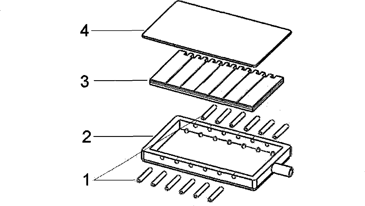
[0036] see figure 1 and figure 2 The cell electrofusion chip consists of a shell 2, a microelectrode array chip 3 fixed in the shell, a sample inlet and outlet conduit 1 connecting the inside and outside of the shell, and a silicon glass sheet 4 packaged on the surface of the shell.

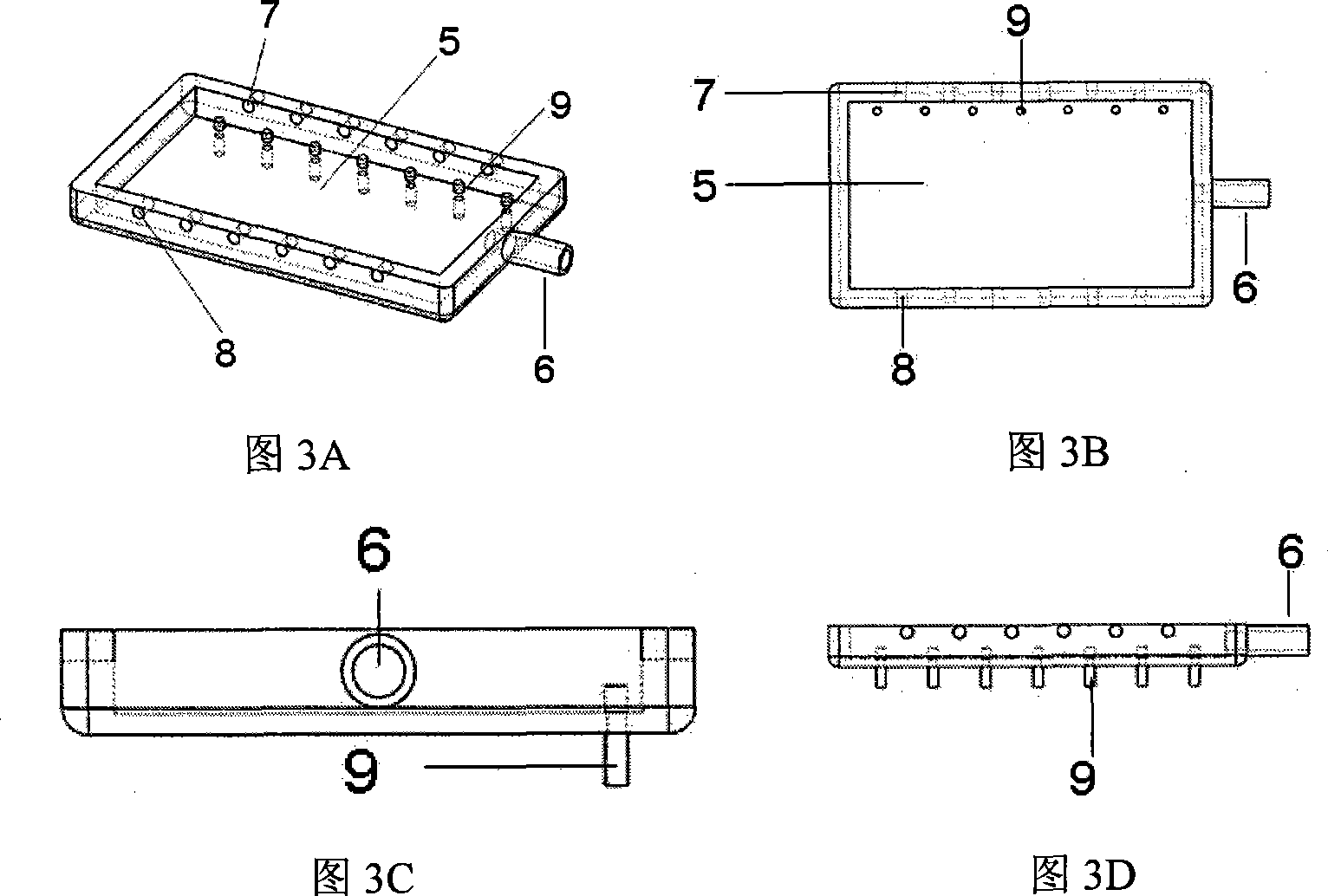
[0037] For the structure of the housing see image 3 , image 3 A is a perspective view of the casing. image 3 B is the top view of the shell, image 3 C is the right side view of the case, image 3 D is the front view of the shell, the center of the shell 2 is an inner cavity 5 for accommodating the chip, the bottom has pins 9 corresponding to the microelectrode array of the chip, and the two side walls have a sample inlet 7 and a sample outlet 8, and in the shell 2. A cylinder 6 is arranged on the outside to facilitate the removal of the whole device.

[0038] For the structure of the microelectrode array chip see Figure 4 A. Figure 4 B and Figure 4 C, the microelectrode array chi...


PUM


Abstract

The invention discloses a cell-electrofusion chip of continuous flow based on silicone structure of an insulator and a processing technology thereof. The cell-electrofusion chip comprises a shell, a microelectrode array chip fixed in the shell, a sample input and output pipe communicating with the inside and the outside of the shell, and a silicone glass sheet encapsulated on the surface of the shell. The microelectrode array chip consists of a siliceous basal layer, a silicon dioxide insulating layer, a low-resistivity silicon electrode layer and a silicon dioxide protective film in turn from down to up. Using the micro machining technology, a groove is etched on the low-resistivity silicon electrode layer of silicon materials on the insulator till the silicon dioxide insulating layer forms a microelectrode structure. In virtue of microscale and arrangement of microchannel, external electric signals forms gradient field with sufficient intensity and increases cell-electrofusion efficiency. At the same time, a linear type microchannel constructed on the chip contributes for the flow of cell suspension and reduces cell adhesion in flow movement as low as possible. The development of the cell-electrofusion experiment of continuous flow can approximate to provide fusion cells with unlimited quantity.

Description

technical field [0001] The invention relates to a device for electrical fusion of biological cells. Specifically, the present invention relates to a chip that provides cell electrofusion, provides and generates the electric field strength and electric field gradient required for cell queuing, electroporation, and fusion, and relates to the precise control of cells in cell electrofusion and the efficient fusion of cells, suitable for Genetics, animal and plant distant hybrid breeding, developmental biology, drug screening, monoclonal antibody preparation, mammalian cloning and other fields. Background technique [0002] Biological cells can form new cells through fusion, which is of great significance in the basic field of modern biomedical engineering. Cell fusion technology has gone through several stages of development such as biological, chemical and physical induction. In the 1980s, with the development of electronic information technology, cell electrofusion technolog...

Claims


Application Information

Patent Timeline
IPC IPC(8): C12M1/42
CPCC12M35/02
Inventor 杨军胡宁郑小林侯文生罗洪艳曹毅杨静夏斌许蓉徐涛
Owner CHONGQING UNIV
Why Eureka
Try Eureka