
Method for preparing fine line flexible circuit board with high peeling strength

A flexible circuit board and manufacturing method technology, which are applied in secondary processing of printed circuits, ion implantation plating, improvement of metal adhesion of insulating substrates, etc., can solve the problems of extremely high substrate requirements, limited market application, and high overall cost , to achieve the effect of high material utilization, improved drilling quality and high peel strength

Active Publication Date: 2009-02-25
GUANGZHOU FANGBANG ELECTRONICS
View PDF2 Cites 33 Cited by
  • Summary
  • Abstract
  • Description
  • Claims
  • Application Information

AI Technical Summary

Problems solved by technology

The conductive layer (planting layer) is directly formed on the surface of the substrate, and then electroplating is completed. This process has extremely high requirements for the substrate, especially for flexible copper clad laminates. At present, only KAPTON EN produced by DuPont in the world can really meet the requirements, and the peel strength is relatively high. Low, the overall cost is particularly high, which limits the market application of this technology

Method used


Image

  • Method for preparing fine line flexible circuit board with high peeling strength
  • Method for preparing fine line flexible circuit board with high peeling strength
  • Method for preparing fine line flexible circuit board with high peeling strength

Examples


Embodiment 1

[0027] A method for manufacturing a thin circuit flexible circuit board with high peel strength, comprising the following steps:

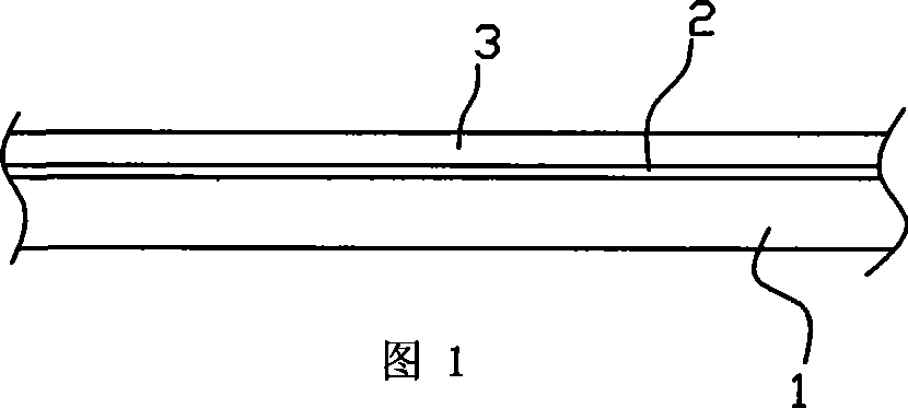
[0028] 1), the formation of thin copper with aluminum foil (see Figure 1): select aluminum foil (1) as the carrier, the thickness of the aluminum foil is 8um to 50um, preferably 8um or 12um or 20um or 35um or 50um, and the width is 100mm to 1000mm, Preferably 100mm or 250mm or 500mm or 750mm or 1000mm, vacuum sputtering a layer of sputtered copper layer (2) that can improve the peel strength of thin copper and the carrier on one side of the aluminum foil, the thickness of the sputtered copper layer is 100mm angstroms to 300 angstroms, preferably 100 angstroms or 150 angstroms or 300 angstroms, and then roll-shaped electroplating thin copper layer (3) on the sputtered copper layer, the thickness of the thin copper layer is 2um to 35um, preferably 2um or 5um or 9um or 12um.

[0029] 2) Production of copper-clad laminates with aluminum foil (see Figu...

Embodiment 2

[0037] The difference from the above implementation is that in step 1), aluminum alloy foil or nickel foil or nickel alloy foil is selected as the carrier, and the following procedures are the same as in the first embodiment.

Embodiment 3

[0039] The difference from the first embodiment lies in step 1), the sputtered metal layer (2) is manganese or iron or tungsten or nickel or chromium or nickel-chromium alloy, and the following steps are the same as the first embodiment.

[0040]The present invention adopts the sputtering method to form the sputtering layer, the thickness of the sputtering layer will not change due to the roughness of the carrier metal foil, and finally ensures the uniformity of the peeling strength. In addition, the sputtering layer is made of one kind of metal. The present invention does not need to consider the two characteristics of high peel strength and easy peeling at high temperature. Considering the actual circuit board manufacturing process requirements, only high peel strength is considered, which improves the quality more effectively. The stability of the carrier metal foil is corroded after drilling in the circuit board processing process, which has the effect of improving the qual...


PUM

PropertyMeasurementUnit
Thicknessaaaaaaaaaa
Thicknessaaaaaaaaaa
Thicknessaaaaaaaaaa

Abstract

The invention relates to a method for producing a fine line flexible circuit board with high racking strength, including the following steps: selecting a metal foil as the carrier, vacuum sputtering a layer of sputtering metal level, which can improve the racking strength of the thin copper and the carrier, on one side of the metal foil, then coiling the planting thin copper layer on the sputtering metal level; selecting a film matrix which is coated with B stage modified epoxy or B stage acrylics or polyester film of TPI resin or polyimide film or liquid crystal polymer film on one side or on double sides; placing the thin copper layer with metal foil, release paper layer, silicon rubber layer, Teflon layer, stainless steel layer on surface of one side or double sides of the matrix in sequence from inside out; and then pressing the thin copper layer with metal foil carrier on surface of one side of the matrix or on surfaces of the double sides of the matrix separately. Comparing with the prior art, the equality of the racking strength is effectively ensured at last, and the processing control is simple, the affinity between the matrix and the thin copper layer is good, the racking strength is high, the yield rate is high, and the cost for processing is low; the method is suitable for processing circuit boards with small-bore, and has high reliability; the electroplated layer is uniform and is suitable for producing a large amount of fine line products; the method can be used for producing flexible circuit boards with broad width, the utility ratio of the material is high and the efficiency is high.

Description

technical field [0001] The invention relates to a method for manufacturing a thin circuit flexible circuit board with high peeling strength. Background technique [0002] Driven by the miniaturization of electronic products and the rapid development of liquid crystal display electronic products, the application market of flexible circuit boards has been rapidly expanded. As its main raw material, flexible copper clad laminates are currently in a state of rapid growth in both technology and market. In LCD driver IC, it plays the role of bearing IC chip, circuit connection and insulation support. Its main features are high fine lines and high position accuracy of installation leads. To produce circuit boards with high fine lines, thin copper foil (thickness less than 9 micron copper foil) flexible copper clad laminate is the key material. [0003] The invention patent named ultra-thin copper foil with carrier and printed circuit board, the application date is December 14, 2...

Claims


Application Information

Patent Timeline
IPC IPC(8): H05K3/38C23C14/34C23C14/14
Inventor 苏陟
Owner GUANGZHOU FANGBANG ELECTRONICS
Features
  • Generate Ideas
  • Intellectual Property
  • Life Sciences
  • Materials
  • Tech Scout
  • Unparalleled Data Quality
  • Higher Quality Content
  • 60% Fewer Hallucinations
Learn More