Electrostatic chuck

An electrostatic chuck and electrostatic attraction technology, applied in the field of microelectronics, can solve the problems that the insulating layer 1 cannot obtain enough heat and cannot heat up.

Active Publication Date: 2009-03-04
BEIJING NAURA MICROELECTRONICS EQUIP CO LTD
View PDF0 Cites 8 Cited by
  • Summary
  • Abstract
  • Description
  • Claims
  • Application Information

AI Technical Summary

Problems solved by technology

[0009] However, in practical applications, since the base 3 is usually made of aluminum, and aluminum itself is a good conductor of heat conduction, and the heater 2 and the base 3 are only bonded together by a thin layer of silica gel, and cannot Form an effective thermal insulation layer between the

Method used


Image

  • Electrostatic chuck
  • Electrostatic chuck
  • Electrostatic chuck

Examples


Embodiment Construction

[0023] In order to enable those skilled in the art to better understand the technical solutions of the present invention, the electrostatic chuck provided by the present invention will be described in detail below with reference to the accompanying drawings.

[0024] The present invention fully considers the influencing factors of heat conduction, and blocks the heat generated by the heater from conducting to the base by setting a heat insulating layer between the heater and the base, so that the processed devices such as wafers on the electrostatic chuck have A sufficiently large heating rate and good zone temperature control can further improve the uniformity of processing (for example, etching) of processed devices such as wafers.

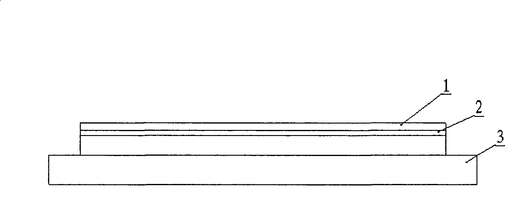
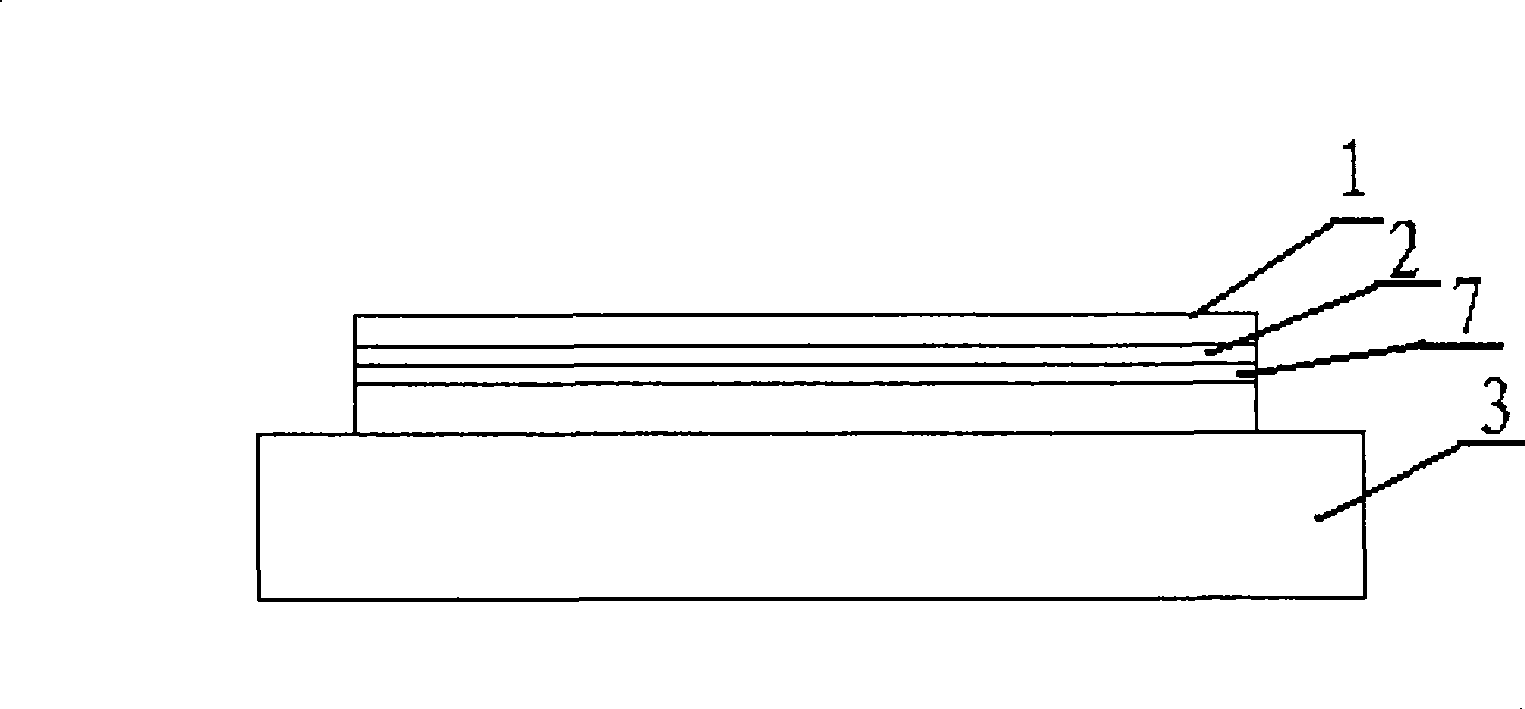
[0025] see image 3 , The electrostatic chuck in the first embodiment of the present invention includes an insulating layer 1 , a heater 2 , a heat insulating layer 7 and a base 3 in order from top to bottom.

[0026] where, similar to figure ...


PUM


Abstract

The invention relates to an electrostatic chuck used for the semiconductor process, and in particular discloses an electrostatic chuck used for fixing parts to be processed in the processing of semiconductor by virtue of electrostatic attraction. The electrostatic chuck comprises an insulated layer, a heater, a base and a thermal insulating layer arranged between the heater and the base. And the parts to be processed are placed on the insulated layer, the base is used for supporting the insulated layer and the heater, and the thermal insulating layer is used for obstructing the conduction of heat generated by the heater to the base. By virtue of the thermal insulating layer, most of heat generated by the heater is only conducted to the insulated layer, thus leading to sufficiently big rate of temperature increase of such parts to be processed as the electrostatic chuck and the wafers on the chuck and causing the parts to be processed of the wafers and the like so as to reach the predetermined temperature in an extremely short time in the processing of semiconductor (especially in a semiconductor etching process), and finally the processing uniformity (for example, etching) of such parts to be processed as wafers is further enhanced.

Description

technical field [0001] The invention relates to the technical field of microelectronics, in particular to an electrostatic chuck used in semiconductor processing technology. Background technique [0002] In the integrated circuit (IC) manufacturing process, especially in the plasma etching (ETCH), physical vapor deposition (PVD), chemical vapor deposition (CVD) and other processes, in order to fix, support and transfer the wafer (Wafer) etc. To process devices, to avoid movement or dislocation of the processed devices, an Electro Static Chuck (ESC) is often used. [0003] Electrostatic chucks use electrostatic attraction to fix processed devices such as wafers, which can be divided into two types: Coulomb and Johnson-Rahbek. Since the electrostatic chuck uses electrostatic attraction instead of traditional mechanical methods to fix wafers and other processed devices, it can reduce damage to wafers and other processed devices caused by mechanical reasons such as pressure and...

Claims


Application Information

Patent Timeline
IPC IPC(8): H01L21/683C23C14/50C23C16/458B23Q3/08
Inventor 彭宇霖
Owner BEIJING NAURA MICROELECTRONICS EQUIP CO LTD
Why Eureka
Try Eureka