Method for measuring carrier mobility of organic semiconductor by using evanescent wave as excitation source

A carrier mobility, organic semiconductor technology, applied in the measurement of electricity, measurement devices, measurement of electrical variables, etc., can solve the problems of inaccuracy, difficulty in carrier mobility, and difficulty in measuring the thickness of photogenerated carrier thin layers. , to achieve the effect of improving accuracy and reducing measurement error

Inactive Publication Date: 2009-03-11
JILIN UNIV
View PDF0 Cites 11 Cited by
  • Summary
  • Abstract
  • Description
  • Claims
  • Application Information

AI Technical Summary

Problems solved by technology

Although the thickness of the excitation layer can be controlled to a certain extent by adjusting the intensity of the excitation light source, it is very imprecise, and the thickness of the thin layer of photogenerated carriers is difficult to measure; at the same time, in order to minimize the thickness of the excitation thin layer, it is necessary to reduce the current the number of generated carriers, thus causing great difficulty in obtaining accurate and reliable carrier mobility

Method used


Image

  • Method for measuring carrier mobility of organic semiconductor by using evanescent wave as excitation source
  • Method for measuring carrier mobility of organic semiconductor by using evanescent wave as excitation source
  • Method for measuring carrier mobility of organic semiconductor by using evanescent wave as excitation source

Examples


Embodiment 1

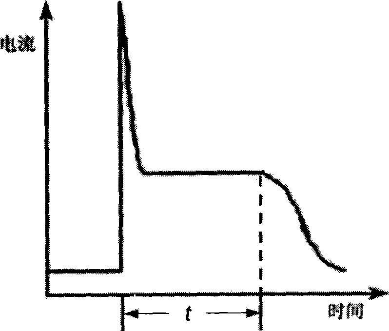
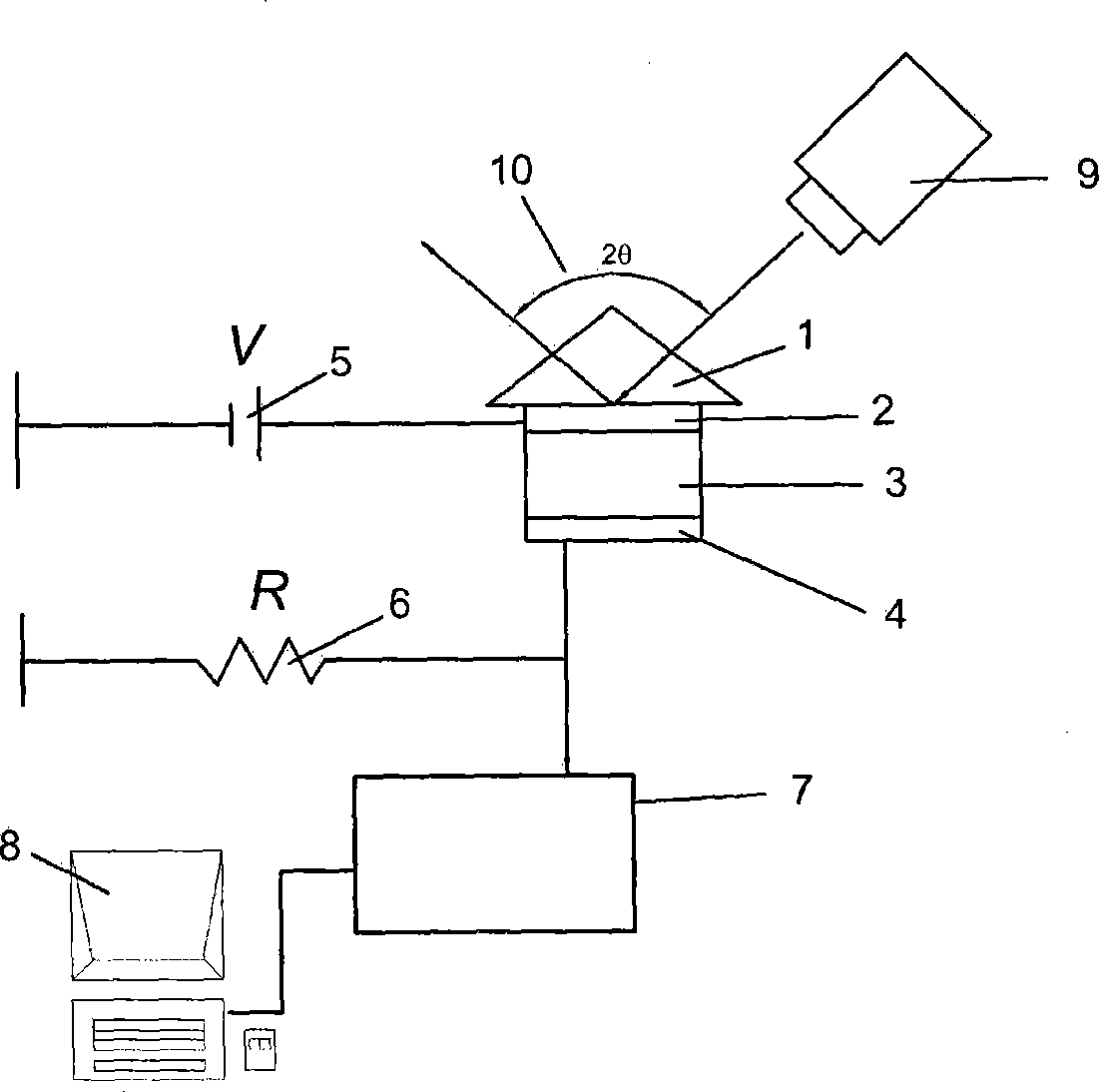
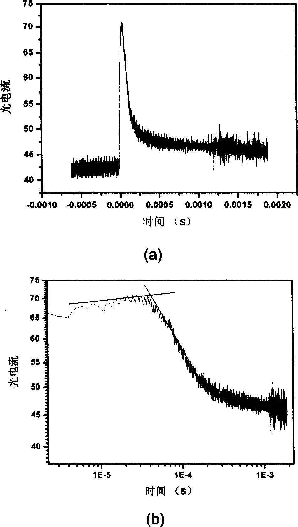
[0042] Firstly, according to the content of the invention, the instruments needed for the test system are selected. Among them, the Nd:YAG laser with a pulse width of 6 ns is selected as the light source (Contimuum Minilite II, the single pulse energy range of the excitation light is about 10uJ~5mJ, and the wavelength is 532nm); an adjustable optical goniometer (Rigakn, Japan) ; DC stabilized voltage, the output range is 0 ~ 200V; adjustable rheostat, the resistance range is 0 ~ 10 6 ohm; storage oscilloscope (Tektronix 4054), the frequency is 500MHz and microcomputer, etc., according to the attached figure 2 The composition of the carrier mobility measurement setup is shown.

[0043] The purpose of this example is to measure the hole mobility of a polyphenylene vinylene conjugated polymer (MEH-PPV) organic semiconductor film. Therefore, the MEH-PPV film was used as the active layer of the test sample.

[0044] First, 20 mg of MEH-PPV was dissolved in 1 ml of chloroform (C...


PUM


Abstract

The invention relates to a method for measuring the mobility of an organic semiconductor material current carrier by utilizing an evanescent wave generated by a total internal reflection method as an excitation source. The method comprises the steps that: firstly, an organic semiconductor material film with thickness d is prepared on a semitransparent electrode and the vapor deposition of a layer of metal electrode is carried out; later, pulsed light is led to the surface of the semitransparent electrode by incidence at the angle that Theta<1> is more than or equal to Theta <c> and less than or equal to 90 DEG, the evanescent wave generated by the total internal reflection generates a hole-electron pair in the organic semiconductor material film; the hole or the electron carries out drift motion toward a cathode or an anode under the action of an electric field formed by externally applied voltage U and finally collected by the cathode or the anode, and a transient photocurrent is collected by a signal collection part, thus determining the time t for the hole or the electron to transit across the organic semiconductor material film and then obtaining the mobility of the organic semiconductor material current carrier, namely, Mu equals to d<2> divided by Ut. The method can control the generation quantity of photon-generated carriers by adjusting the lightness of the exciting light, thus improving the measurement accuracy of the mobility of the current carriers.

Description

technical field [0001] The invention belongs to the technical field of carrier mobility testing of organic semiconductor materials, and in particular relates to a method for measuring carrier mobility of organic semiconductor materials by using evanescent waves generated by a total internal reflection method as an excitation source. technical background [0002] Organic semiconductor materials are widely used in optoelectronic devices such as light-emitting diodes, solar cells, and field-effect transistors due to their advantages such as easy regulation of molecular structure, simple preparation process, and large-area flexible devices. Carrier mobility (usually represented by .) is an important basic parameter of organic semiconductor materials, and is closely related to the performance of organic semiconductor optoelectronic devices. Carrier mobility is defined as the ratio of the average drift velocity V of free carriers (electrons or holes) to the applied electric field ...

Claims


Application Information

Patent Timeline
Patent Type & Authority Applications(China)
IPC IPC(8): G01R31/00
Inventor 田文晶徐蔚青徐斌唐彬周印华
Owner JILIN UNIV
Why Eureka
Try Eureka