Composite passivated reflection reducing membrane for crystalline silicon solar cell and preparation thereof

A crystalline silicon solar cell and solar cell technology, applied in the field of solar cells, can solve the problems of performance deterioration, no advantage, poor quality of silicon wafers, etc., and achieve excellent passivation, simple and feasible preparation process, and good anti-reflection effects

Inactive Publication Date: 2009-03-11
INST OF ELECTRICAL ENG CHINESE ACAD OF SCI +1
View PDF1 Cites 8 Cited by
  • Summary
  • Abstract
  • Description
  • Claims
  • Application Information

AI Technical Summary

Problems solved by technology

However, due to the poor quality of silicon wafers used in industry, their performance will be further deteriorated after high temperature treatment (usually above 1000°C). Therefore, the silicon dioxide passivation layer produced by this high temperature oxidation is not industrially acceptable. Be applicable
[0004] Titanium dioxide film usually has a refractive index of about 2.0. Titanium dioxide film with a thickness of 80nm has a good anti-reflection effect on crystalline silicon solar cells, but unfortunately, titanium dioxide film has no passivation effect on the silicon surface
Therefore, from the perspective of anti-reflection, silicon nitride has no advantage over titanium dioxide

Method used


Image

  • Composite passivated reflection reducing membrane for crystalline silicon solar cell and preparation thereof

Examples


Embodiment 1

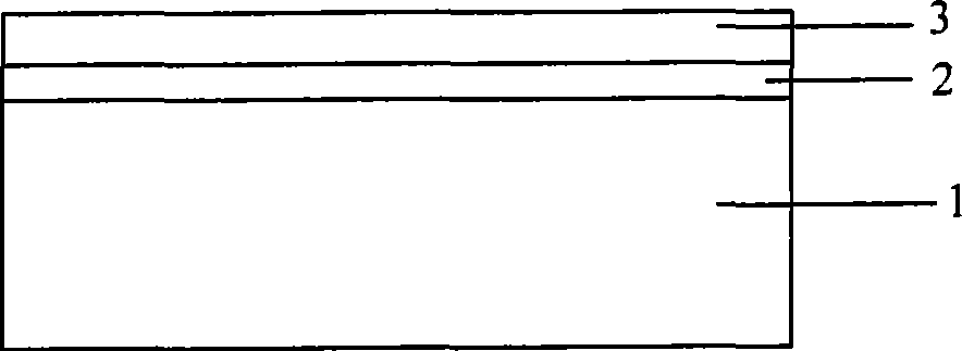
[0015] An amorphous silicon / titanium dioxide composite passivation anti-reflection film, wherein the thickness of the amorphous silicon layer directly deposited on the light-facing surface of the solar cell to play a passivation role is 25 nanometers, and the amorphous silicon layer is deposited on the The thickness of the anti-reflection titanium dioxide layer is 80 nanometers.

Embodiment 2

[0017] A method for preparing an amorphous silicon / titanium dioxide composite passivation anti-reflection film, comprising: adopting a chemical vapor deposition (PECVD) process to deposit and prepare a 5-nanometer thick amorphous silicon layer on a solar cell, and then depositing a 5-nanometer thick amorphous silicon layer on the amorphous silicon A 90nm-thick titanium dioxide layer is deposited on the crystalline silicon layer by using an atmospheric pressure chemical vapor deposition (APCVD) process.

Embodiment 3

[0019] A method for preparing an amorphous silicon / titanium dioxide composite passivation anti-reflection film, comprising: adopting a chemical vapor deposition (PECVD) process to deposit and prepare a 50-nanometer thick amorphous silicon layer on a solar cell, and then depositing a 50-nanometer thick amorphous silicon layer on the amorphous silicon A 70nm-thick titanium dioxide layer is deposited on the crystalline silicon layer by a thermal spraying process.


PUM

PropertyMeasurementUnit
thicknessaaaaaaaaaa
thicknessaaaaaaaaaa
refractive indexaaaaaaaaaa

Abstract

The invention relates to a composite passivation antireflective film used for a crystal silicon solar cell. The invention is characterized in that the composite passivation antireflective film is composed of a layer of amorphous silicon layer (2) and a layer of titanium dioxide layer (3), wherein the amorphous silicon layer (2) is directly deposited on the irradiation surface of a solar cell (1) and plays the role of surface passivation, and the titanium dioxide layer (3) is deposited on the amorphous silicon layer (2) and plays the role of reducing the reflection of light of the battery. The invention also relates to a method for preparing the passivation antireflective film, and the method comprises the following steps: firstly, the amorphous silicon layer (2) is deposited and prepared on the solar cell (1) by adopting a PECVD (plasma enhanced chemical vapor deposition) process, and then the titanium dioxide layer is deposited on the amorphous silicon layer (2) by adopting an APCVD (atmospheric pressure chemical vapor deposition) process, or the titanium dioxide layer (3) is deposited on the amorphous silicon layer (2) by adopting a thermal spraying process.

Description

technical field [0001] The invention relates to the field of solar cells, in particular to a composite passivation antireflection film for crystalline silicon solar cells and a preparation method thereof. Background technique [0002] In order to improve the conversion efficiency of solar cells, on the one hand, it is usually necessary to make an optical anti-reflection film (anti-reflection film) on the light-facing surface of the solar cell to ensure that as much light as possible is not reflected and enters the interior of the solar cell to be absorbed; On the other hand, it is necessary to prepare a surface passivation film on the surface of the solar cell to reduce the recombination center generated by the surface defect state, thereby increasing the photocurrent. [0003] The silicon dioxide produced by high-temperature thermal oxidation on the surface of the silicon wafer has a good passivation effect on the surface of the silicon wafer, and this silicon dioxide passi...

Claims


Application Information

Patent Timeline
Patent Type & Authority Applications(China)
IPC IPC(8): H01L31/02H01L31/0203H01L31/0232H01L31/048H01L31/052H01L31/20H01L31/0216
CPCY02E10/52Y02P70/50
Inventor 赵雷王文静
Owner INST OF ELECTRICAL ENG CHINESE ACAD OF SCI
Why Eureka
Try Eureka