

Probe-induced surface plasma resonance lithographic device and method
A technology of surface plasmon and resonant light, which is applied in the direction of microlithography exposure equipment, photolithography process exposure equipment, measurement equipment, etc., can solve the problems of lithography equipment not appearing, super-resolution mask thermal fatigue, super-resolution performance degradation, etc. Problems, easy maintenance and upgrades, improved positioning accuracy, and low laser power
- Summary
- Abstract
- Description
- Claims
- Application Information
AI Technical Summary
Problems solved by technology
Method used
Image

Examples
Embodiment Construction
[0064] The specific details and operation methods of the present invention will be described in detail below with reference to the accompanying drawings and examples, but the protection scope of the present invention should not be limited thereto.
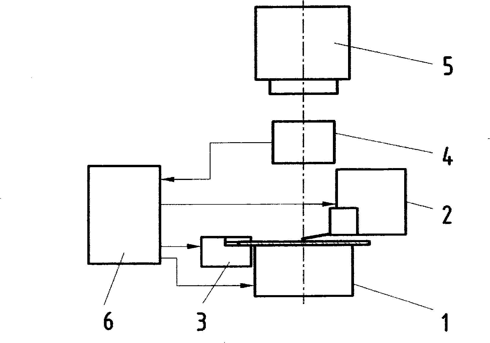
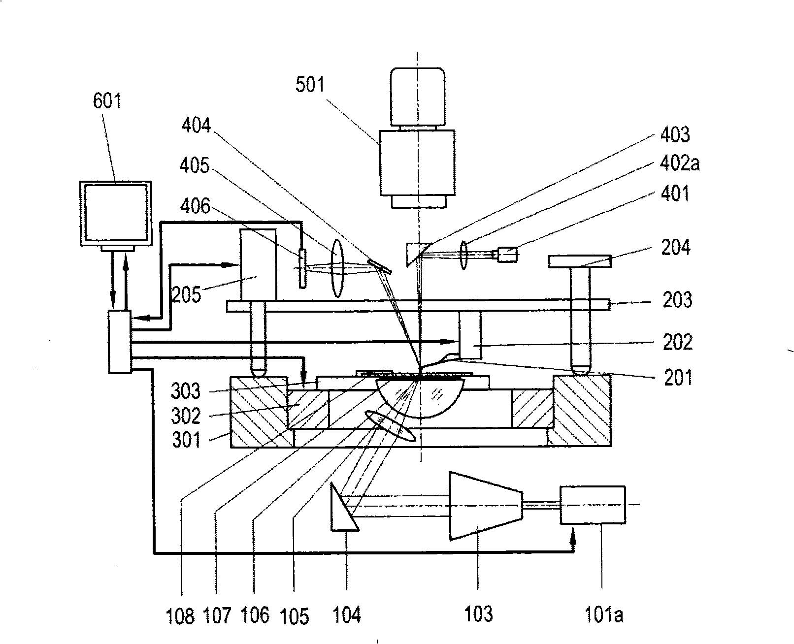
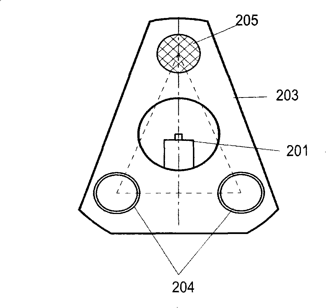
[0065] see first figure 1 , figure 2 and image 3 , figure 1 It is a schematic diagram of the system composition of the probe-induced surface plasmon resonance lithography device of the present invention; figure 2 It is a structural schematic diagram of the first preferred embodiment of the present invention; image 3 yes figure 2 The top view of the probe control device 2; it can be seen from the figure that the probe-induced surface plasmon resonance lithography device of the present invention consists of a surface plasmon excitation device 1, a probe control device 2, a sample stage 3, a probe state detection device 4, Composition of optical microscope 5 and control system 6: see figure 2 and image 3 , the structure ...
PUM
 Abstract
Description
Claims
Application Information