Photoelectric position detector with high-sensitivity

A photoelectric position, high-sensitivity technology, used in circuits, electrical components, semiconductor devices, etc., can solve the problems that the sensitivity cannot meet the requirements of its application, the response band width, etc., and achieve the effect of convenient application, good linearity and simple structure.

Inactive Publication Date: 2009-04-22
INST OF PHYSICS - CHINESE ACAD OF SCI
View PDF0 Cites 13 Cited by
  • Summary
  • Abstract
  • Description
  • Claims
  • Application Information

AI Technical Summary

Problems solved by technology

[0005] The purpose of the present invention is: to overcome the deficiency that the sensitivity of the existing photodetector cannot meet the requirements of its application, thereby providing a photoelectric position detect

Method used


Image

  • Photoelectric position detector with high-sensitivity
  • Photoelectric position detector with high-sensitivity
  • Photoelectric position detector with high-sensitivity

Examples


Embodiment 1

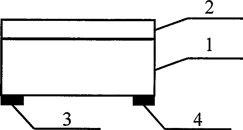
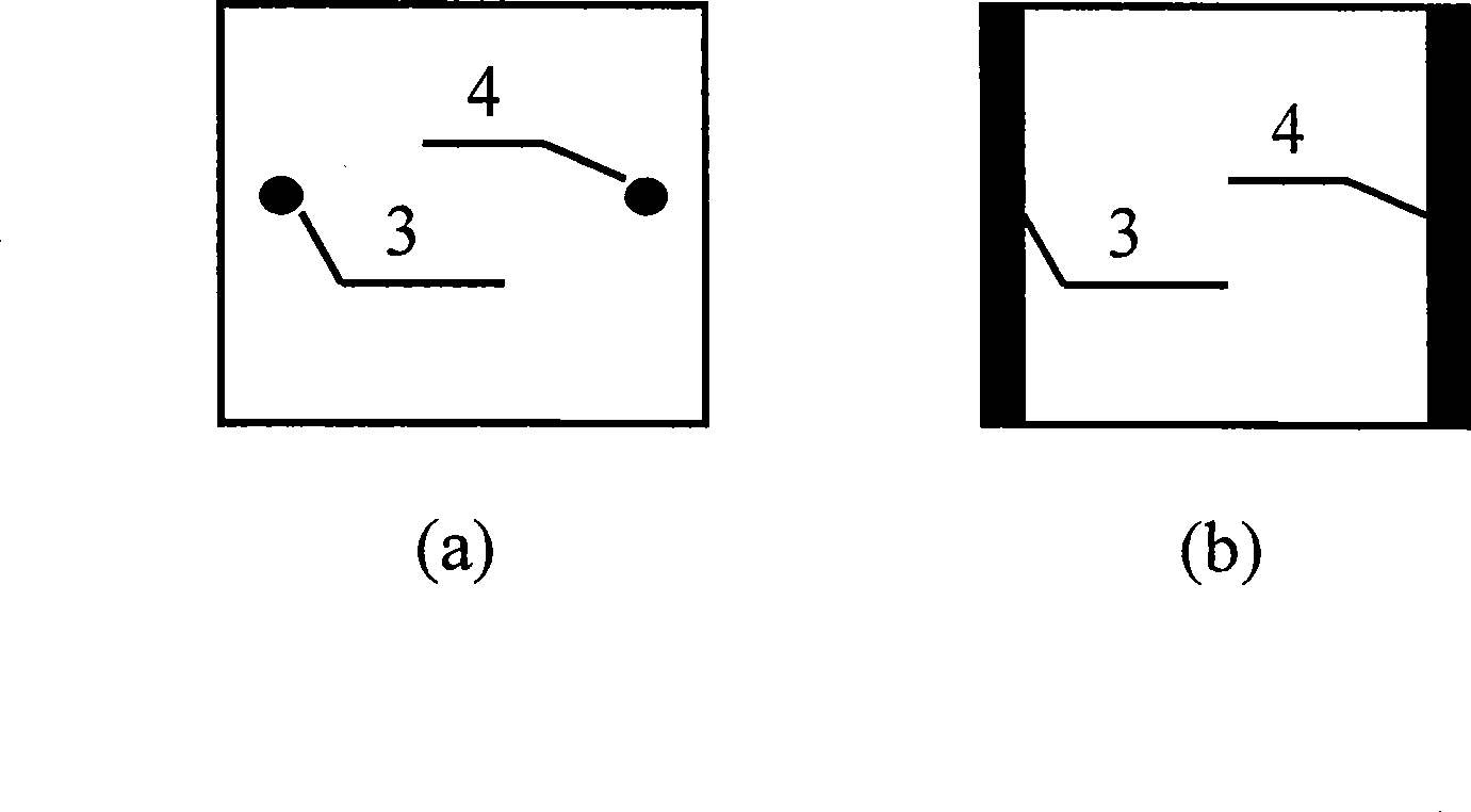
[0023] refer to figure 1 , in conventional laser molecular beam epitaxy equipment, laser molecular beam epitaxy technology is used to directly epitaxially grow a 100nm thick TiN thin film layer 2 on a 2-inch Si substrate 1 to form a TiN-Si two-layer heterojunction sample. A 2-inch TiN-Si sample was cut into a 10 mm x 10 mm square. On the outer surface of the Si substrate 1 of the TiN-Si two-layer heterojunction sample, with the center of the two sides, the first electrode 3 and the second electrode 4 (such as figure 2 As shown in a), the distance between the first electrode 3 and the second electrode is 8mm, that is, it is prepared as a photoelectric position detector whose working mode is voltage mode.

[0024] The measurement results are as follows:

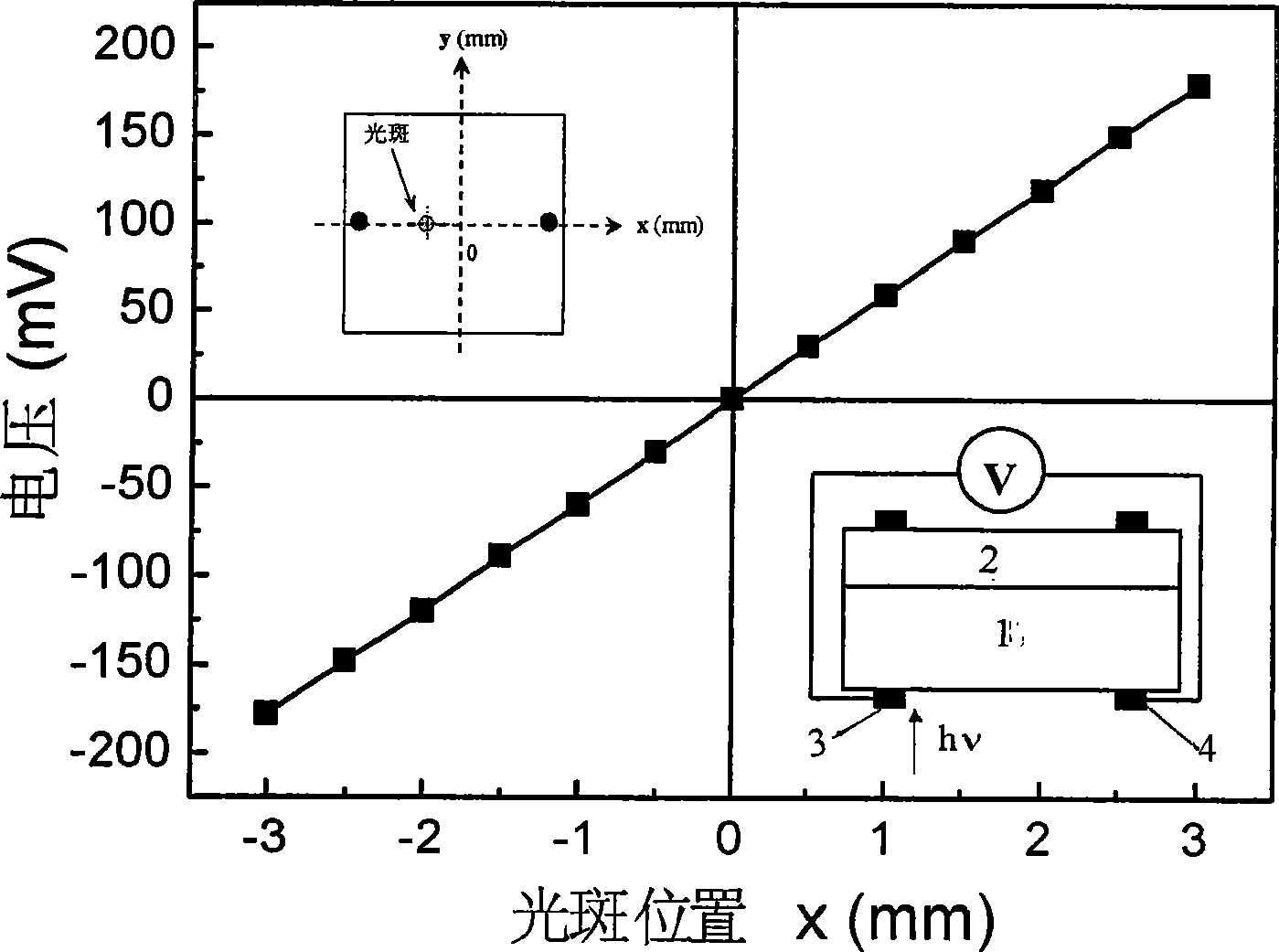
[0025] Use a 10mW HeNe laser (wavelength 632.8nm) as the light source, use a diaphragm with a diameter of 0.5mm to limit the spot area, and scan the spot between the first electrode 3 and the second electrode 4 on the Si sub...

Embodiment 2

[0027] Using the photoelectric position detector produced in Example 1, an excimer pulsed laser with a wavelength of 308 nm was used instead of HeNe laser as the light source for measurement. Figure 4 It is a TiN-Si heterojunction photoelectric position detector. When an excimer pulse laser with a wavelength of 308nm is used to scan in a straight line between two points on the Si surface electrode, the relationship between the output voltage between the first electrode 3 and the second electrode 4 and the position of the light point, The inset is a schematic diagram of the specific measurements.

Embodiment 3

[0029] Using laser molecular beam epitaxy technology, a 1nm-thick TiN film layer 2 is directly epitaxially grown on a 2-inch Si wafer 1 to form a TiN-Si two-layer heterojunction sample. A 2-inch TiN-Si sample was cut into a 10 mm x 10 mm square. At the center of the two sides of the Si substrate 1 square surface, prepare a gold first electrode 3 and a second electrode 4 with a diameter of about 0.5mm (such as figure 2 As shown in a), a photoelectric position detector prepared as a voltage mode.

[0030] When a light spot shines on the surface of the detector, measure the voltage between the first electrode 3 and the second electrode 4 with a voltmeter, or connect a voltage source between the first electrode 3 and TiN, so that TiN and Si form The Schottky diode works in the reverse bias state, and the current between the first electrode 3 and the second electrode 4 is measured, and the position of the light spot can be identified according to the measured voltage or current. ...


PUM

PropertyMeasurementUnit
Thicknessaaaaaaaaaa

Abstract

The invention provides a photoelectric position detector with high sensitivity. The detector comprises a Si substrate and two electrodes. TiN film is epitaxially grown on the Si substrate by a film making method; the electrodes are respectively prepared on both sides of the Si substrate by a film coating method or a welding method. When a light spot illuminates the surface of the detector, a voltmeter is used for measuring a voltage between the electrodes; or a voltage source is connected between the electrodes and the TiN to cause a schottky diode composed of the TiN and the Si to work under a reverse bias condition, and then the current between the electrodes is measured; therefore, the position of the light spot can be determined according to the measured voltage or the current. The photoelectric position detector has the advantages of simple structure, good linearity and high sensitivity, can directly detect the voltage or the current without an additional amplifying circuit, and can detect millimicrosecond level fast-pulse signals.

Description

technical field [0001] The invention relates to a position detector, in particular to a high-sensitivity photoelectric position detector based on titanium nitride and silicon heterojunction. Background technique [0002] The idea of ​​the photoelectric position detector was proposed by Wallmark as early as 1957. Its basic structure is covered by a high-conductivity layer film on the semiconductor substrate to form a Schottky diode structure, and a built-in electric field is formed in its interface region. . When a small spot of light is irradiated on the detector, a large number of photogenerated electrons and hole pairs will be generated near the spot. Under the action of the built-in field, the electrons and holes diffuse in space, and the current-carrying on the side of high conductance The carriers will quickly reach a new equilibrium distribution, making it an equipotential body, and the carriers on the semiconductor side will form a concentration gradient distribution...

Claims


Application Information

Patent Timeline
IPC IPC(8): H01L31/109
Inventor 邢杰吕惠宾何萌金奎娟刘国珍周岳亮杨国桢
Owner INST OF PHYSICS - CHINESE ACAD OF SCI
Why Eureka
Try Eureka