Production technology for anti-reflection film of solar cell

A production process and anti-reflection coating technology, applied in the manufacture of circuits, electrical components, final products, etc., can solve the problems of easy process fluctuations, burn-through, poor blocking ability of harmful impurities, etc., and achieve enhanced high-temperature penetration blocking effect, Effects of reduced radiation damage and wide process temperature range

Inactive Publication Date: 2009-05-13
浙江弘晨光伏能源有限公司
View PDF0 Cites 7 Cited by
  • Summary
  • Abstract
  • Description
  • Claims
  • Application Information

AI Technical Summary

Problems solved by technology

At present, the industrial production process in the industry adopts the method of PECVD plasma chemical vapor deposition, and the silicon wafer is placed in the plasma field to directly deposit a layer of Si on the surface of the silicon wafer. x N y , Thin film, this is a conventional and mature anti-reflection film growth process, usually the thickness of the film layer is 80±3nm, the refractive index is 2.05±0.02, and the anti-reflection effect of the anti-reflection film on the incident light can reach 5~ 6%, but due to the faster growth rate (0.8nm / s), the film texture is looser, not only prone to PN junction "burn-through" phenomenon, but also harmful impurities (such as Na + , Fe + ) has poor blocking ability, which makes it easy to produce process fluctuations in the battery manufacturing process

Method used


Image

  • Production technology for anti-reflection film of solar cell
  • Production technology for anti-reflection film of solar cell
  • Production technology for anti-reflection film of solar cell

Examples


Embodiment Construction

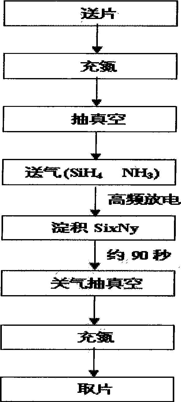
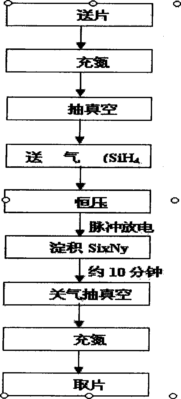
[0016] Such as figure 2 Shown, the concrete production technological process of the present invention is as follows:

[0017] 1. Clean single crystal silicon wafer: clean the silicon wafer that has been diffused to form a PN junction and has been cleaned by plasma edge removal and PSG (phosphosilicate glass) to keep the surface of the silicon wafer dry and free of water stains;

[0018] 2. Inserting the wafer: put the clean and dry silicon wafer N + The layer is vertically inserted into the carrier graphite boat (note that the whole boat must be filled, if it is insufficient, it must be replaced with a companion piece), and then sent into the reaction chamber at a speed of 600mm / min;

[0019] 3. Constant temperature: the boat is sent into the reaction chamber. The ambient temperature in the reaction chamber is 480°C. Due to the influence of the cold end effect, the temperature will drop by 60°C. In order to ensure that the film density in the entire reaction chamber is unifo...


PUM


Abstract

The invention discloses an improved SixNy antireflection coating growth technique which can effectively reduce the reflection loss of surface incident light, simultaneously enhance the compactness of a surface antireflection coating and enhance the blocking effect on harmful impurities, such as Na<+>, Fe<+>, etc. The power of a medium-high frequency plasma source in the growth technique process is 800W, the environmental temperature in a reaction chamber is 480 DEG C, the flow rate of silane is 300sccm, the flow rate of ammonia maintains the technological process parameter of 1,800sccm, and the advance and retreat speed of a carrying boat of a technological silicon wafer is 600mm / min, thereby ensuring the grown coating to be capable of carrying out the timely passivation and annealing (carrying out the passivation and the annealing during the growth), therefore, the compactness thereof is enhanced and the surface radiation damage to PN junction can be repaired timely and effectively. The growth technique is applicable to the production of crystalline silicon solar cells.

Description

technical field [0001] The invention relates to a production process of an anti-reflection film for solar cells, in particular to the improvement of the production process for a silicon nitride anti-reflection film on the surface of a crystalline silicon solar cell suitable for large-scale industrial production. The invention can produce Si with good compactness, good uniformity and good adhesion. x N y Anti-reflective coating. Background technique [0002] With the increasing awareness of environmental protection, international and domestic development and utilization of renewable energy, especially solar energy, has drawn more and more attention. The cost of photovoltaic power generation has dropped by two orders of magnitude in the past 30 years, and the photovoltaic industry has maintained an annual growth rate of 40% to 50% in the past 5 years. From 2001 to 2006, the global solar cell output increased from 386MW to 2500MW, an increase of 5.48 times, with an annual in...

Claims


Application Information

Patent Timeline
Patent Type & Authority Applications(China)
IPC IPC(8): H01L31/18
CPCY02P70/50
Inventor 向小龙何旭梅王保军郦晓苗蒋伟平何珊
Owner 浙江弘晨光伏能源有限公司
Why Eureka
Try Eureka