Double-frequency band inductor multiplexing radio frequency CMOS low-noise amplifier

A low-noise amplifier and dual-band technology, applied to DC-coupled DC amplifiers, differential amplifiers, improved amplifiers to reduce noise effects, etc., can solve the problems of increasing chip footprint and large power consumption, and achieve chip area and power saving little effect

Inactive Publication Date: 2009-05-13
EAST CHINA NORMAL UNIVERSITY
View PDF0 Cites 17 Cited by
  • Summary
  • Abstract
  • Description
  • Claims
  • Application Information

AI Technical Summary

Problems solved by technology

Zhenbiao Li et al. published the paper "A Dual—Band CMOS Front—End With Two Gain Modes for Wireless LAN Applications", which reported a dual-band RF low-noise amplifier with high gains in both frequency bands, reaching 30dB respectively. and 25dB, see

Method used


Image

  • Double-frequency band inductor multiplexing radio frequency CMOS low-noise amplifier
  • Double-frequency band inductor multiplexing radio frequency CMOS low-noise amplifier
  • Double-frequency band inductor multiplexing radio frequency CMOS low-noise amplifier

Examples


Embodiment

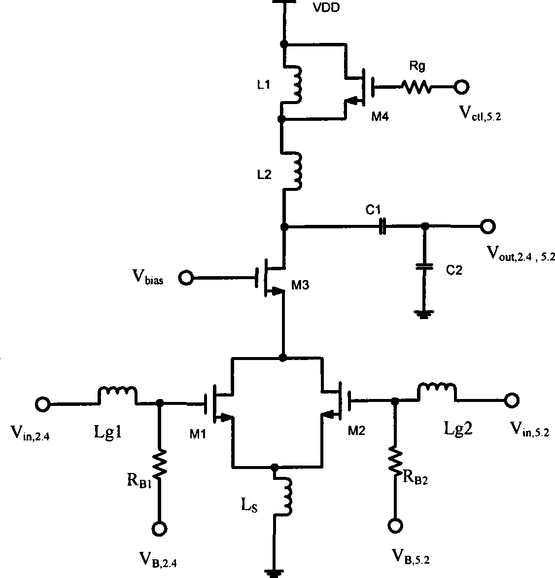
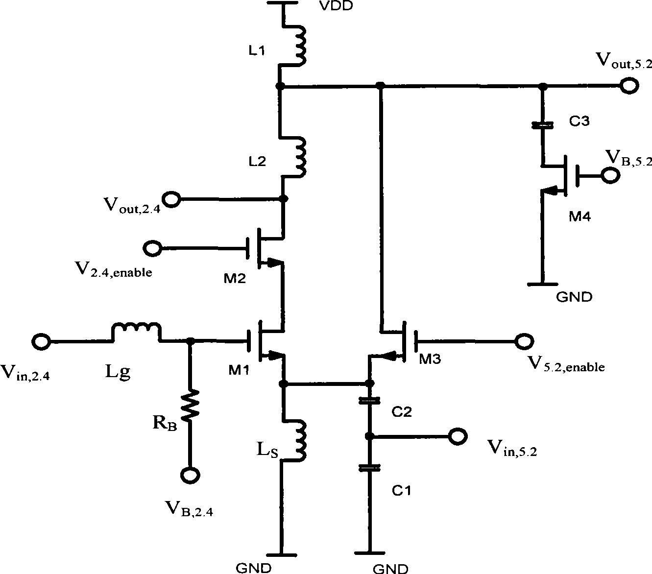
[0018] This embodiment has the same figure 2 The circuit shown is exactly the same circuit structure. The specifications and circuit parameters of the components used in this embodiment are listed as follows:

[0019] The width-to-length ratios of the first MOS transistor M1, the second MOS transistor M2, the third MOS transistor M3, and the fourth MOS transistor M4 are 120 μm / 0.13 μm, 100 μm / 0.13 μm, 130 μm / 0.13 μm, and 150 μm / 0.13 μm;

[0020] The first inductance L g , the second inductance L s , the inductances of the third inductor L1 and the fourth inductor L2 are 8.885nH, 1.166nH, 2.766nH, 7.657nH respectively;

[0021] The capacitance values ​​of the first capacitor C1, the second capacitor C2, and the third capacitor C3 are 35fF, 300fF, and 50fF respectively;

[0022] Resistance R B 2kΩ;

[0023] The bias terminal of the amplifier that amplifies the 2.4GHz signal V B,2.4 The voltage is 0.9V or 0V;

[0024] The enable terminal V of the amplifier that amplifies...


PUM

PropertyMeasurementUnit
Inductanceaaaaaaaaaa
Resistanceaaaaaaaaaa

Abstract

A radio-frequency CMOS low noise amplifier of dual-band inductance multiplexing belongs to the technical field of radio-frequency low noise amplifiers. Based on a dual-band low noise amplifier in the prior art, the pattern of amplifying a 5.2 GHz signal is changed into a common-gate amplification mode; an inductor is dislodged; a 5.2 GHz enable circuit consisting of MOS transistors is added; and a 5.2 GHz output signal is output from a 5.2 GHz signal output terminal separated from a 2.4 GHz signal output terminal. The amplifier has the advantages of low noise, low power consumption, small area and the like, and is especially suitable for serving as a front-end amplifier in a wireless communication device.

Description

technical field [0001] The invention relates to a radio-frequency CMOS low-noise amplifier with dual-band inductance multiplexing, and belongs to the technical field of radio-frequency low-noise amplifiers. Background technique [0002] In recent years, with the rapid development of radio frequency integrated circuits, the use of wireless communication products in daily life has become increasingly frequent: 900MHz GSM mobile phones, 2.4GHz Bluetooth communications, 4.9GHz public safety communication systems, 5.2GHz wireless LANs, etc. An important part of the front end of the wireless receiver module in these products is the Radio Frequency Low Noise Amplifier (RFLNA for short). Its function is to amplify the weak signal received through the antenna, and at the same time reduce the noise of the RF low noise amplifier itself as much as possible, and increase the gain as much as possible, so that the subsequent modules of the receiver can process it. Since the RF low-noise a...

Claims


Application Information

Patent Timeline
IPC IPC(8): H03F3/45H03F1/26
Inventor 马和良陈磊赖宗声张润曦雷奥何伟徐萍张勇李斌
Owner EAST CHINA NORMAL UNIVERSITY
Why Eureka
Try Eureka