
Device for space-modulating atomic layer chemical vapour deposition epitaxial growth and method thereof

A chemical vapor deposition and epitaxial growth technology is applied to the device and field of spatial modulation atomic layer chemical vapor deposition epitaxial growth, and can solve the problems of reducing film deposition rate, reducing equipment utilization rate, occurrence of parasitic reactions, etc.

Inactive Publication Date: 2009-06-03
INST OF SEMICONDUCTORS - CHINESE ACAD OF SCI
View PDF0 Cites 7 Cited by
  • Summary
  • Abstract
  • Description
  • Claims
  • Application Information

AI Technical Summary

Problems solved by technology

The problem with this method is that due to pipeline resistance, part of the gas stagnates, and the lagging part of the raw material gas will still undergo parasitic reactions; to solve this problem, some people introduce carrier gas purge between raw gas switching, but this It reduces the film deposition rate and reduces equipment utilization

Method used


Image

  • Device for space-modulating atomic layer chemical vapour deposition epitaxial growth and method thereof

Examples


example

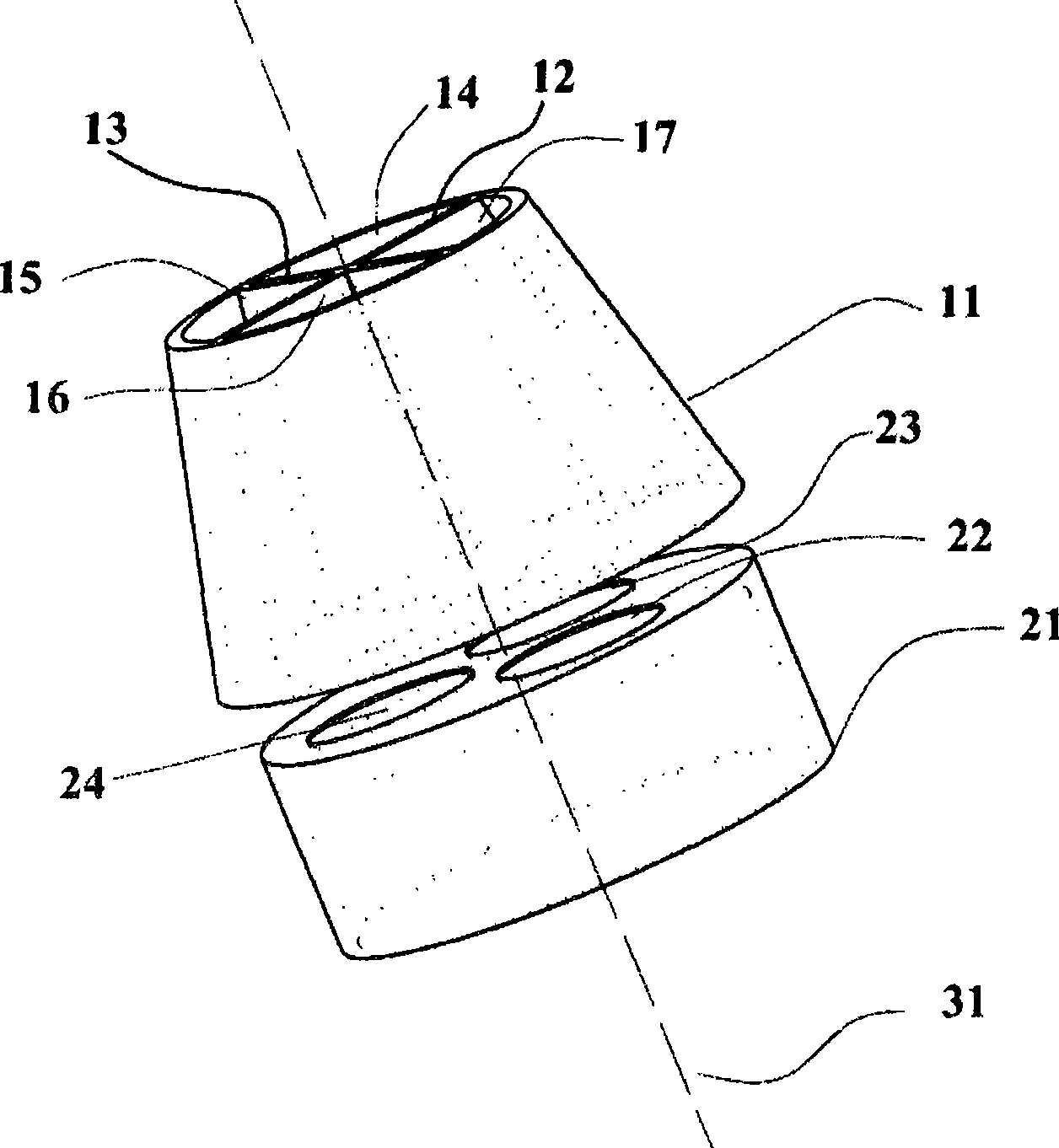
[0048] Different from traditional air intake awnings, partitioned air intake awnings are mainly composed of a hollow barrel-shaped part 11 . The barrel-shaped one is divided into four mutually independent and mutually equivalent regions 14, 15, 16 and 17 by two partitions 12 and 13. Each of these four zones functions the same as a traditional air intake hood. That is to say, various raw material gases required for material growth can be introduced from each zone. Moreover, the same raw material gas or different raw material gases are simultaneously fed into the four subregions.

[0049] Take aluminum nitride (AlN) as an example where the growth parasitic reaction is very serious. In the process of growing, figure 1 The air inlet hood 11 shown can be assigned as follows. Partition 14 passes trimethylaluminum (TMAl), partition 16 passes ammonia (NH 3 ), both partition 15 and partition 17 pass carrier gas (hydrogen H 2 or nitrogen N 2 ). Among them, TMAl and NH imported f...

Embodiment 1

[0066] Embodiment one: see attached figure 1 Shown is a schematic diagram of the reaction chamber structure of a spatially modulated atomic layer chemical vapor deposition system. Comprising a multi-partition 14, 15, 16 and 17 intake tent head 11 and a rotatable base 21 that is dug with grooves 22-24 for placing substrates, and an accommodating rotating base and intake tent Head, the cavity that isolates the reaction gas from the air.

[0067] Use example one: adopt the reaction chamber structure of embodiment one, when preparing high crystal quality zinc oxide (ZnO) film deposition, a kind of raw material gas diethylzinc enters from inlet pipe through partition 14, and another kind of raw material gas oxygen enters from The inlet pipe enters through partition 16, and the carrier gas argon enters from the inlet pipe through partitions 15 and 17. In this way, the raw material gas diethylzinc and oxygen are independently transported in the process of approaching the substrate,...


PUM


Abstract

The invention relates to a device for space-modulating atomic layer chemical vapor deposition epitaxial growth. The device is characterized by comprising an air-intake shower and a base wherein, the air-intake shower is barrel-shaped and the interior of the air-intake shower is divided into a plurality of regions, and each region is an air-intake nozzle of feed gas; the base is a column and is provided with a plurality of circular grooves thereon, the circular grooves are used for placing a substrate; the diameter of the base is less than or equal to the diameter of the air-intake shower and the base can rotate; wherein, the air-intake shower is positioned at the side of base, the surface of which is provided with the circular groove; a certain distance exists between the air-intake shower and the base; one end of the air-intake shower, which is close to the base, is an air outlet; and the other end, which is far from the basement, is an air outlet.

Description

technical field [0001] The invention relates to a spatially modulated atomic layer chemical vapor deposition epitaxial growth method, in particular to a method for separating various raw material gases from each other in space through a specially designed gas inlet device, and then through methods such as rotation or translation The substrate of the epitaxial material is successively passed through the "space modulation" method of the space covered by different types of raw material gases, which can avoid parasitic reactions between the raw material gases, high raw material gas utilization efficiency, and high growth rate. Preparation of semiconductor epitaxial materials ( Especially group III nitride materials, including AlN, GaN and InN and their alloy compounds) atomic layer chemical vapor deposition epitaxial growth method. Background technique [0002] Chemical vapor deposition technology (Chemical Vapor phase Deposition referred to as CVD) is an important semiconductor...

Claims


Application Information

Patent Timeline
Patent Type & Authority Applications(China)
IPC IPC(8): C30B25/02
Inventor 朱建军杨辉王怀兵
Owner INST OF SEMICONDUCTORS - CHINESE ACAD OF SCI
Learn More