Punch through effect enhanced type silicon photo transistor

A punch-through effect, enhanced technology, applied in circuits, electrical components, semiconductor devices, etc., can solve the problems of low SNR, low gain, large dark current, etc., to improve photoelectric conversion gain, improve photoelectric conversion gain, high photoelectric conversion gain effect

Inactive Publication Date: 2009-06-03
长春长光圆辰微电子技术有限公司
View PDF0 Cites 8 Cited by
  • Summary
  • Abstract
  • Description
  • Claims
  • Application Information

AI Technical Summary

Problems solved by technology

Due to the recombination of the two-terminal phototransistor in the space charge region at the base-emitter PN junction, when the incident light power is very low, the gain is very low; in addition, the low incident light power also causes the charging time of the emitter junction capacitance to be very short Long, so the gain-bandwidth product and SNR become very small, which limits the high-speed application of this phototransistor
[0004] Although the three-terminal phototransistor has achieved some success in improving the gain and response speed, the shot noise introduced by the base bias current is also amplified by the transistor at the same time. Therefore, when the base current is much larger than the photogenerated current, the SNR will change. is very low, which severely limits the detection sensitivity of the three-terminal phototransistor in low-light conditions
Silicon through-base phototransistors not only have high gain and fast response rate performance, but also overcome the shortcomings of compound through-base phototransistors that are difficult to integrate
However, whether it is a compound substrate or a silicon substrate through base phototransistor, their dark current is relatively large, and they are not fully compatible with standard commercial CMOS processes.

Method used


Image

  • Punch through effect enhanced type silicon photo transistor
  • Punch through effect enhanced type silicon photo transistor
  • Punch through effect enhanced type silicon photo transistor

Examples


Embodiment 1

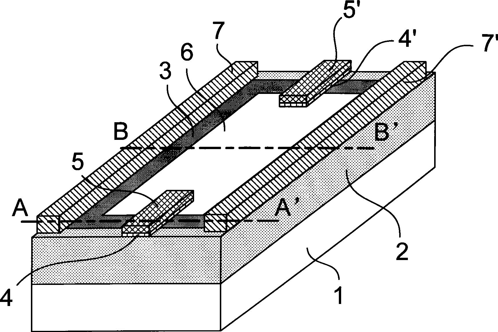
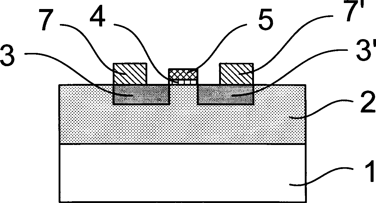
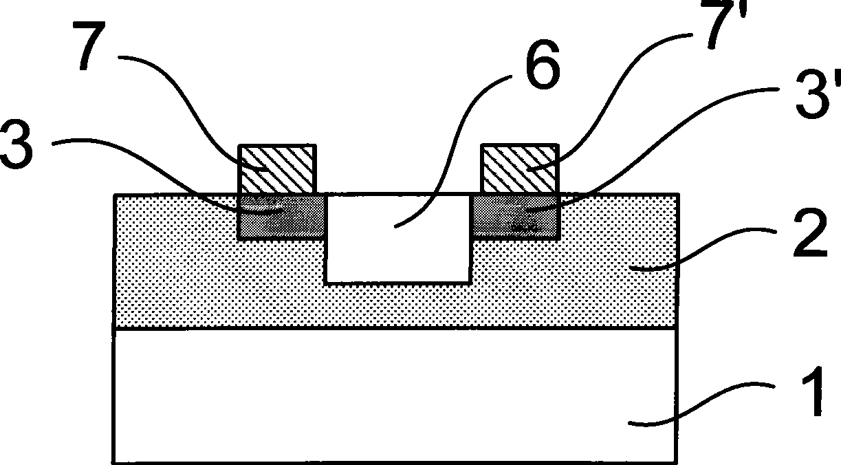
[0053] Since the punch-through effect enhanced silicon phototransistor of the present invention is fully compatible with standard CMOS technology, it can be implemented on any standard CMOS technology line. The specific preparation method will be described below by taking an NPN-type punch-through effect-enhanced silicon phototransistor manufactured by a standard double-well CMOS process with a feature size of 0.5 μm, two layers of polysilicon, and three layers of metal as an example.

[0054] A: Selection of substrate - select a P-type silicon substrate, the substrate resistivity is 15Ω·cm, and the thickness is 100μm;

[0055] B: Formation of the well region—a well is formed by high-energy ion implantation and thermal propulsion. Since it is to make an NPN phototransistor, the P well is used as the base area of ​​the device, that is figure 1 2 of them. As was implanted, the implantation energy and dose of ion implantation were 100keV and 5×10 12 cm -2 . After advancing ...


PUM


Abstract

The invention relates to a punch through effect enhanced type silicon photo transistor which comprises two types which are a NPN type and a PNP type; the silicon photo transistor sequentially comprises a silicon substrate layer, a P pit (or a N pit) layer positioned on the silicon substrate layer, two discrete N type (or P type) heavy doping active areas positioned inside the P pit (or a N pit) layer, a field silicon dioxide layer surrounded by the two N type (or P type) heavy doping active areas, two discrete bar-shaped gate oxide silicon dioxide layers which are arranged at the narrow side of the P pit (or a N pit) layer and on the upper surface of the field silicon dioxide layer, two discrete polysilicon layers that are coated on the gate oxide silicon dioxide layers and have the same shapes as that of the gate oxide silicon dioxide layers, and a bar-shaped metallic electrode layer that is positioned on the upper surface at the wide side of the P pit (or a N pit) layer and is respectively connected with the two discrete N type (or P type) heavy doping active areas from bottom to top. The device can effectively improve photoelectric conversion gain of devices, limit the dark current of devices, and reduce the noise of devices, so as to obtain higher signal-to-noise.

Description

technical field [0001] The invention belongs to the field of semiconductor optoelectronic devices, in particular to a silicon phototransistor with punch-through effect enhancement. Background technique [0002] Semiconductor photodetectors have been widely used due to their excellent performance, tiny size and cheap price, and have penetrated into all aspects of society such as industrial and agricultural production, military technology, daily civilian use, and consumer electronics. Silicon photodetectors are a large class of semiconductor photodetectors. At present, silicon photodetectors that are widely used mainly include PIN photodiodes, APD avalanche photodiodes, and ordinary phototransistors. These photodetectors have disadvantages such as large size, high requirements on the performance of manufacturing materials, high operating voltage, incompatibility between manufacturing process and CMOS process, and difficulty in integrating with peripheral circuits. [0003] T...

Claims


Application Information

Patent Timeline
Patent Type & Authority Applications(China)
IPC IPC(8): H01L31/11
Inventor 常玉春刘欣王玉琦杜国同郭树旭王富昕史中翩
Owner 长春长光圆辰微电子技术有限公司
Why Eureka
Try Eureka