Inductance coupling coil and plasma device

An inductively coupled coil and inductive coupling technology, applied in the directions of plasma, coils, inductors, etc., can solve the problem of uneven plasma density distribution, and achieve the effect of improving distribution uniformity, small difference in chemical reaction rate, and improving quality.

Active Publication Date: 2009-06-24
BEIJING NAURA MICROELECTRONICS EQUIP CO LTD
View PDF0 Cites 7 Cited by
  • Summary
  • Abstract
  • Description
  • Claims
  • Application Information

AI Technical Summary

Problems solved by technology

[0007] In order to solve the problem of uneven distribution of plasma density in the process of semiconductor processing, the invention provides an inductively coupled coil and a plasma device using the inductively coupled coil

Method used


Image

  • Inductance coupling coil and plasma device
  • Inductance coupling coil and plasma device
  • Inductance coupling coil and plasma device

Examples


Embodiment 1

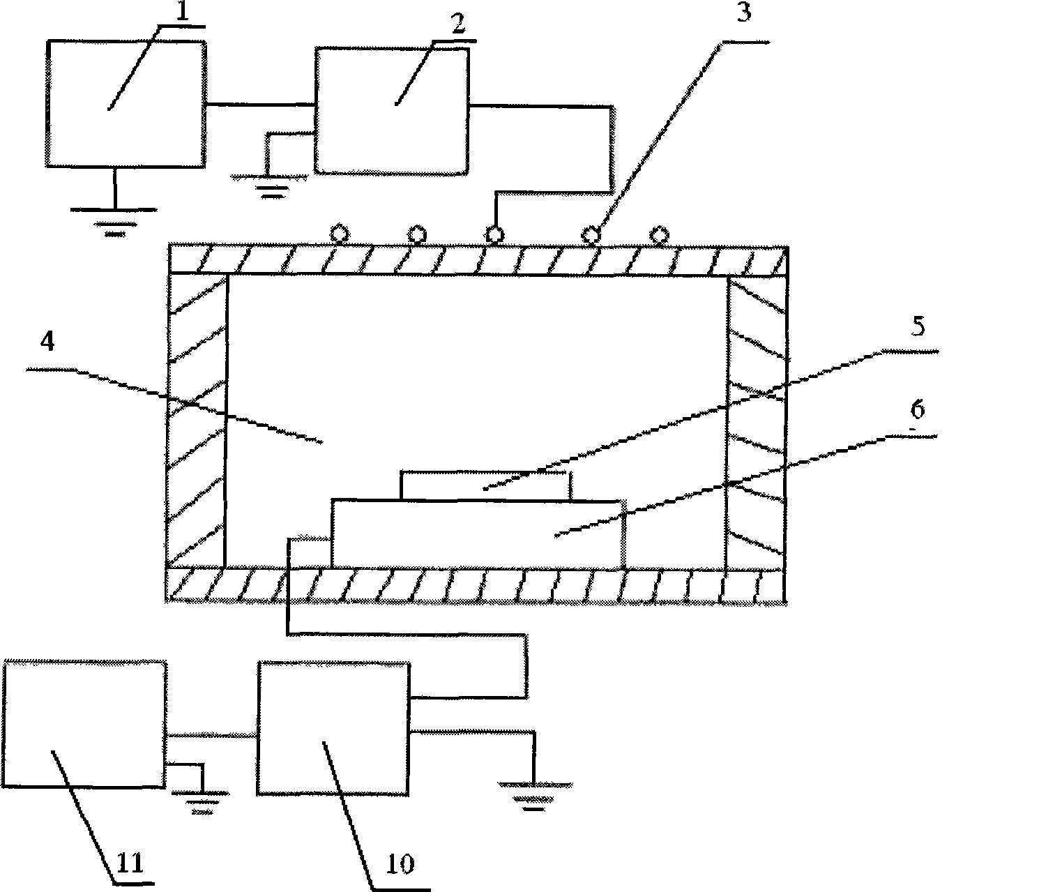
[0027] Such as image 3 As shown in the schematic diagram of the inductive coupling coil structure, the inductive coupling coil includes two identical branches, each branch is composed of an inner coil 7 and an outer coil 8, and the end of the inner coil 7 and the beginning of the outer coil 8 are connected in series by a connecting section 9; The inner and outer coils of the two branches are symmetrically nested and coplanar. The inner coil 7 and the outer coil 8 of each branch are helical and have opposite winding directions, that is, when the inner coil 7 is wound clockwise, the outer coil 8 is wound counterclockwise, or when the inner coil 7 is wound in the opposite direction When clockwise, the winding direction of the outer coil 8 is clockwise. The entire coil is a planar coil.

Embodiment 2

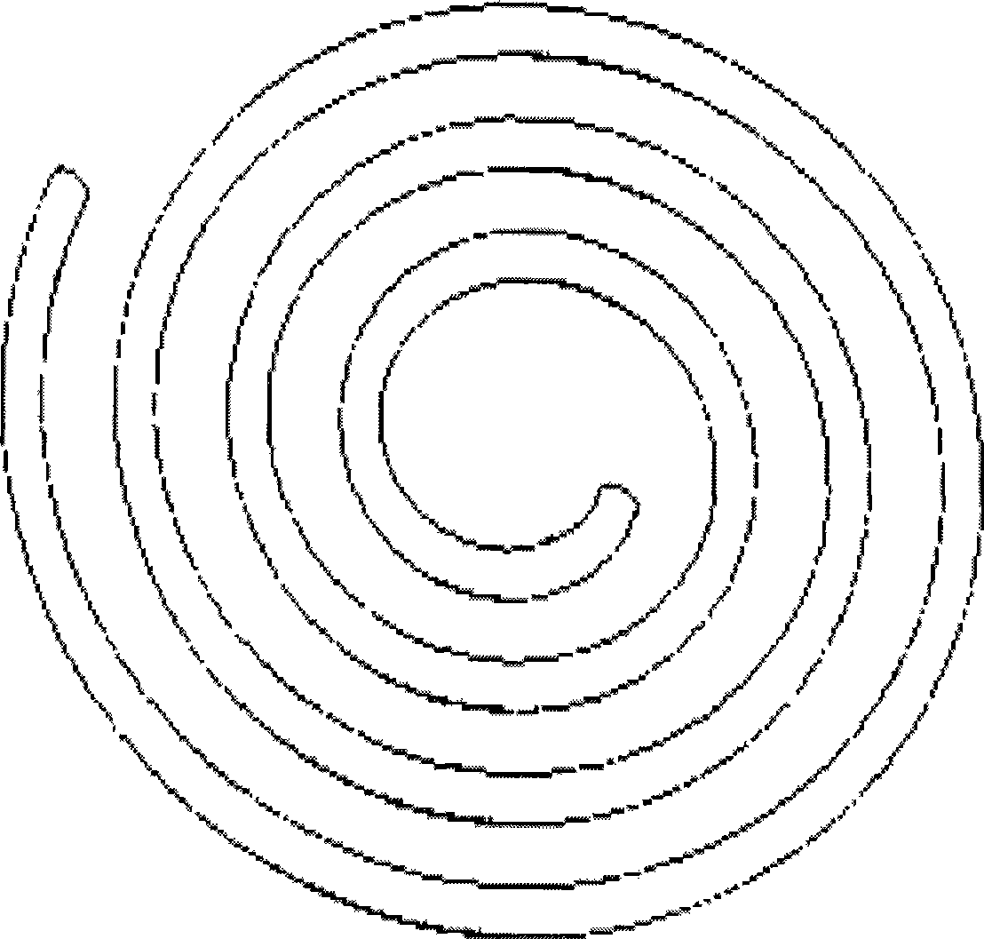
[0029] Such as Figure 4 As shown in the schematic diagram of the structure of the inductive coupling coil, the inductive coupling coil includes two identical branches. Each branch is composed of an inner coil 7 and an outer coil 8. The end of the inner coil 7 and the beginning of the outer coil 8 are connected in series by a connecting section 9. The inner and outer coils of the two branches are symmetrically nested and coplanar. The inner coil 7 of each branch is arc-shaped, and the outer coil 8 is spiral-shaped. The winding directions of the inner coil 7 and the outer coil 8 are opposite, that is, when the inner coil 7 is wound clockwise, the outer coil 8 is wound counterclockwise. Or when the winding direction of the inner coil 7 is counterclockwise, the winding direction of the outer coil 8 is clockwise. The entire coil is a planar coil.

Embodiment 3

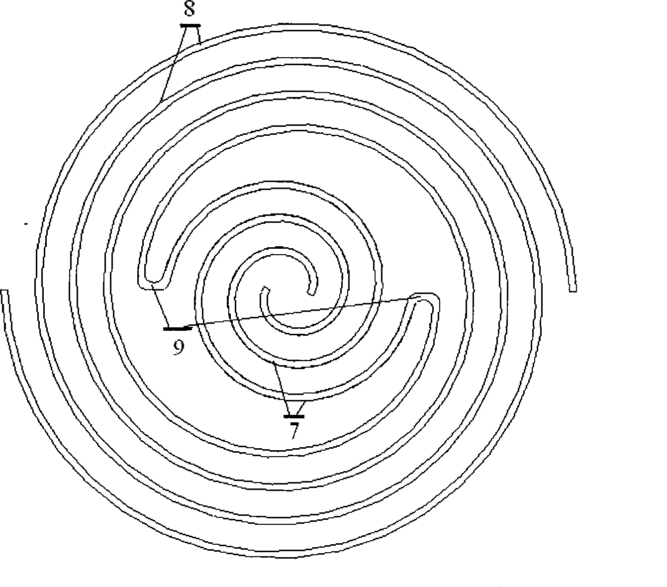
[0031] Such as Figure 5 As shown in the schematic diagram of the structure of the inductive coupling coil, the inductive coupling coil includes two identical branches. Each branch is composed of an inner coil 7 and an outer coil 8. The end of the inner coil 7 and the beginning of the outer coil 8 are connected in series by a connecting section 9. The inner and outer coils of the two branches are symmetrically nested and coplanar. The inner coil 7 of each branched coil is arc-shaped, and the outer coil 8 is formed by connecting multiple arc-shaped coils with successively increasing radii of curvature through the outer coil connecting section 15 in series. The winding directions of the inner coil 7 and the outer coil 8 are opposite, that is, when the inner coil 7 is wound clockwise, the outer coil 8 is wound counterclockwise, or when the inner coil 7 is wound counterclockwise, the outer coil 8 The winding direction is clockwise. The entire coil is a planar coil.


PUM


Abstract

The invention relates to an inductively coupled coil used in the semiconductor machining process, and a plasma device which uses the inductively coupled coil. The key design points lie in that the inductively coupled coil at least comprises two identical branches, and each branch comprises an inner coil (7) and an outer coil (8); the coiling directions of the inner and outer coils are opposite; the tail end of the inner coil (7) is connected with the initial end of the outer coil (8) in series through a connecting segment (9); and the inner and outer coils of each branch are symmetrically nested respectively and are coplanar. When in work, the RF current flowing through the inner coil and the RF current flowing through the outer coil are opposite in direction, so that uniformly distributed electromagnetic fields are generated in a reaction chamber so as to obtain uniformly distributed plasmas; according to the wafer size, a large area of plasmas can be easily obtained through the increase of coil length and number to improve the uniformity of plasmas in the large-area process, so as to achieve less chemical reaction rate differences on the wafer surface and improve the quality of wafer products.

Description

Technical field [0001] The invention relates to an inductive coupling coil and a plasma device, in particular to the technical field in the semiconductor processing process. Background technique [0002] At present, with the rapid development of electronic technology, people have higher and higher requirements for the integration of integrated circuits, which requires companies that produce integrated circuits to continuously improve the processing capabilities of semiconductor wafers. Plasma devices are widely used in the manufacturing process of manufacturing integrated circuits (IC) or MEMS devices. Therefore, the research and development of plasma devices suitable for etching, deposition or other processes is crucial to the development of semiconductor manufacturing processes and equipment. In the research and development of plasma devices for semiconductor manufacturing processes, the most important factors are the ability to work on large substrates in order to increase pro...

Claims


Application Information

Patent Timeline
Patent Type & Authority Applications(China)
IPC IPC(8): H01F5/00H01F38/14H05H1/46H05H1/50H01L21/306
Inventor 韦刚
Owner BEIJING NAURA MICROELECTRONICS EQUIP CO LTD
Why Eureka
Try Eureka