Method for preparing iso-temperature double-buffering layer of sapphire substrate

A sapphire substrate and double buffer layer technology, which is applied in semiconductor/solid-state device manufacturing, electrical components, circuits, etc., can solve the problems of poor growth quality of a single buffer layer, achieve reduced dislocation density, high room temperature mobility, and improved Effect of crystallization quality

Inactive Publication Date: 2009-07-01
深圳市方大国科光电技术有限公司
View PDF0 Cites 6 Cited by
  • Summary
  • Abstract
  • Description
  • Claims
  • Application Information

AI Technical Summary

Problems solved by technology

[0006] The technical problem to be solved by the present invention is to provide a method for preparing double buffer layers of different thicknesses at the same temperature on a sapphire substrate, aiming at the defect of poor growth quality of the above-mentioned single buffer layer in the prior art

Method used


Image

  • Method for preparing iso-temperature double-buffering layer of sapphire substrate
  • Method for preparing iso-temperature double-buffering layer of sapphire substrate
  • Method for preparing iso-temperature double-buffering layer of sapphire substrate

Examples


Embodiment Construction

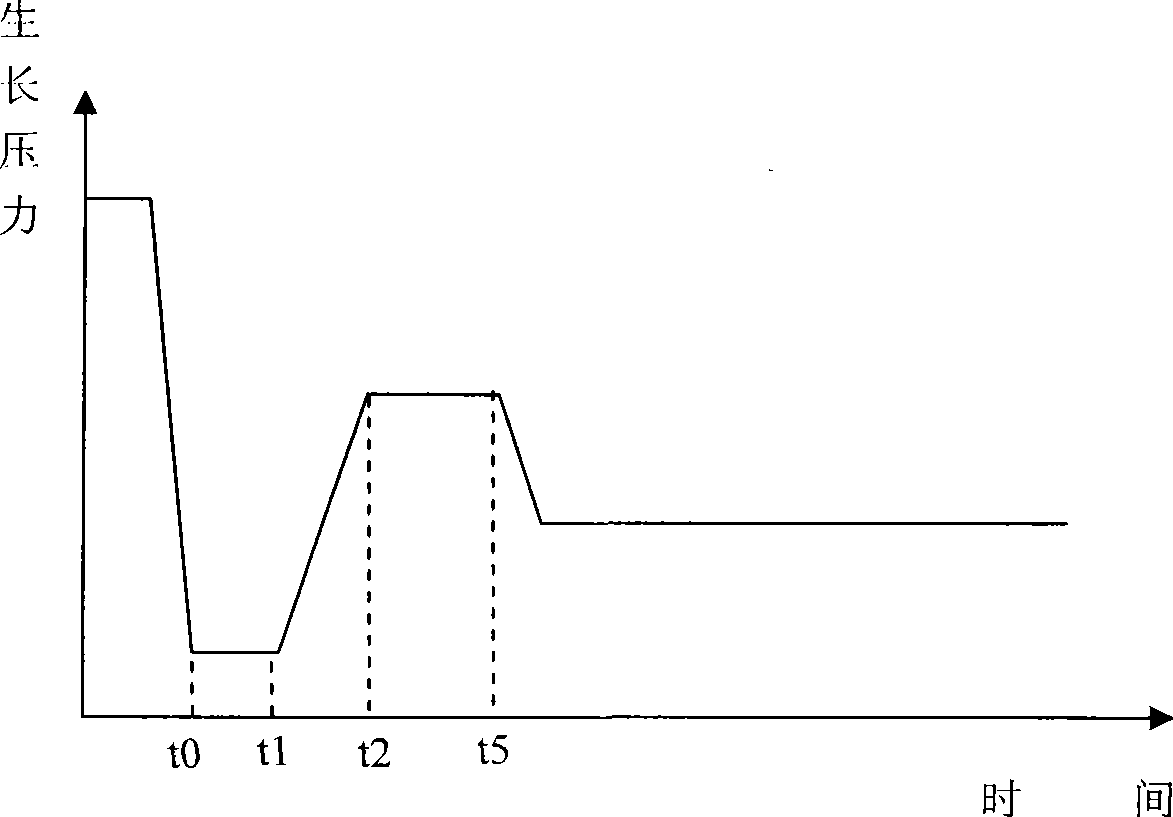
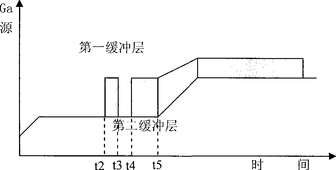
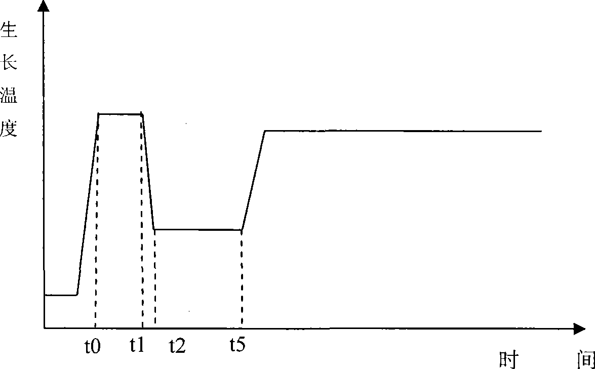
[0026] Such as Figure 1 to Figure 3 Shown is an embodiment of the same-temperature double-buffer layer preparation method for sapphire substrates of the present invention, which introduces low-temperature double-buffer layers with different thicknesses during the epitaxial growth of gallium nitride (GaN) by metalorganic chemical vapor deposition (MOCVD) process technology, in sapphire (Al 2 o 3 ) grow heterogeneous GaN crystals on the substrate, and improve the crystal quality of GaN grown on sapphire. The method mainly includes the following steps:

[0027] Open the vacuum package of the prepared sapphire substrate in the reaction chamber, put it directly into the graphite disk of the MOCVD equipment, and start the program. First, the sapphire substrate is cleaned and pretreated: the reaction chamber is heated to about 1100-1200° C., and the pressure is 100-300 Torr. In this embodiment, the temperature is 1100° C., and the pressure is 100 Torr; and the sapphire surface is...


PUM


Abstract

The invention relates to a processing method of blue stone underlay synthermal double-buffer layers, which comprises the following steps: firstly, putting a blue stone underlay into a reaction cavity for hydrogenating process and getting clean blue stone underlay, secondly, inputting reacting gas into the reaction cavity to create the reacting atmosphere and keeping the temperature and the pressure in a setting range in the cavity, thirdly, inputting beam source containing Ga into the reaction cavity in the first time segment for growing the first buffer layer, fourthly, bypassing the beam source containing Ga and keeping inputting reacting gas in the set time segment after finishing growing the first buffer layer, fifthly, keeping inputting the reacting gas and inputting the beam source containing Ga into the reaction cavity in the second time segment for growing the second buffer layer. In the twice core formation growth, the gap created between crystal nucleus is beneficial for releasing stress created by the mismatching of GaN and Al2O3 crystal lattices, and is beneficial for the transition of GaN three-dimensional growth to two-dimensional growth, thereby forming a plane surface, and improving crystallization quality of GaN.

Description

technical field [0001] The present invention relates to the preparation method of LED (light-emitting diode) chip, more specifically, relate to a kind of LED sapphire substrate isothermal double buffer layer preparation method. Background technique [0002] In the development process of the semiconductor industry, Si and Ge are generally called the first generation semiconductor materials; GaAs, InP, GaP, InAs, AlAs and their ternary and quaternary alloys are called the second generation semiconductor materials; and GaN The representative wide-bandgap semiconductor material (bandgap greater than 2.3eV) has been developed rapidly in recent years, so it is called the third-generation semiconductor material. The third-generation semiconductor materials mainly include SiC, ZnSe, diamond, GaN and GaN-based compounds. It has irreplaceable advantages in radiation resistance, high frequency, high power and high density integrated electronic devices. In addition, due to its unique ...

Claims


Application Information

Patent Timeline
Patent Type & Authority Applications(China)
IPC IPC(8): H01L33/00H01L21/205
Inventor 王新建
Owner 深圳市方大国科光电技术有限公司
Why Eureka
Try Eureka