Method for preparing graphical substrate of GaN-based LED by silicon 001 crystal face
A graphics substrate and graphics technology, applied in semiconductor/solid-state device manufacturing, electrical components, circuits, etc., can solve the problems of high cost and poor quality, and achieve the effect of low cost, good quality and improved crystal quality
- Summary
- Abstract
- Description
- Claims
- Application Information
AI Technical Summary
Problems solved by technology
Method used
Image

Examples
Embodiment Construction
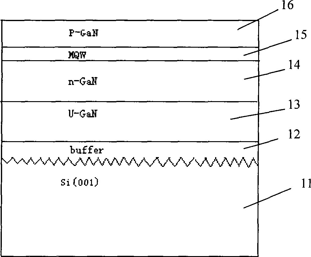
[0027] The method for preparing the pattern substrate of GaN-based LED by using silicon (001) of the present invention is used to prepare a silicon wafer substrate with Si(111) surface, and then the GaN-based LED structure is epitaxially grown on the silicon wafer substrate by the MOCVD method The LED structure includes a buffer layer 12, a u-GaN layer 13, an n-GaN layer 14, a light-emitting layer 15, and a p-GaN layer 16, which are sequentially grown on the substrate 11, such as figure 1 Shown.
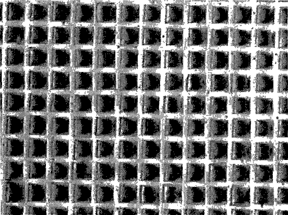
[0028] This method first prepares a mask with patterned openings on Si (001): firstly, SiO is deposited on the silicon (001) by PECVD (plasma enhanced chemical vapor deposition). 2 For the mask layer, the evaporation temperature is 100-400°C and the thickness is 30-500nm. In this embodiment, the evaporation temperature is 200°C, the thickness is 70nm, and the evaporation time is 4 minutes; then, the photolithography technique is used to peel off the part SiO 2 Mask, in SiO 2 The pattern...
PUM
| Property | Measurement | Unit |
|---|---|---|
| Thickness | aaaaa | aaaaa |
| Diameter | aaaaa | aaaaa |
Abstract
Description
Claims
Application Information
 - R&D
- Intellectual Property
- Life Sciences
- Materials
- Tech Scout
- Unparalleled Data Quality
- Higher Quality Content
- 60% Fewer Hallucinations
Browse by: Latest US Patents, China's latest patents, Technical Efficacy Thesaurus, Application Domain, Technology Topic, Popular Technical Reports.
© 2025 PatSnap. All rights reserved.Legal|Privacy policy|Modern Slavery Act Transparency Statement|Sitemap|About US| Contact US: help@patsnap.com