Method for preparing organic semiconductor material rubrene micro-nano wire

An organic semiconductor and rubrene technology, which is applied in semiconductor devices, semiconductor/solid-state device manufacturing, metal material coating processes, etc., can solve the problems of complex preparation process and difficulty in precise control of finished product size, and achieves a simplified preparation process. Effect

Inactive Publication Date: 2009-07-08
SUZHOU INST OF NANO TECH & NANO BIONICS CHINESE ACEDEMY OF SCI
View PDF0 Cites 4 Cited by
  • Summary
  • Abstract
  • Description
  • Claims
  • Application Information

AI Technical Summary

Problems solved by technology

[0004] The present invention aims to provide a method for preparing rubrene micro-nanowires, an organic semiconductor material, which overcomes the problems that the existing preparation process is too complicated and the size of the finished product is difficult to accurately control

Method used


Image

  • Method for preparing organic semiconductor material rubrene micro-nano wire
  • Method for preparing organic semiconductor material rubrene micro-nano wire
  • Method for preparing organic semiconductor material rubrene micro-nano wire

Examples


preparation example Construction

[0024] The present invention designs a novel method for preparing rubrene micro-nanowires, an organic semiconductor material. Compared with previous methods, its outstanding feature is that rubrene is used as a raw material in a clean silicon wafer or a physical vapor transport method. The grown naphthacene single crystal substrate is prepared by vacuum evaporation, and under the conditions of controlling the deposition rate and evaporation time, it is deposited on the semiconductor substrate to form rubrene micro-nano Wire. Necessarily, during the vacuum evaporation process, the semiconductor substrate needs to be kept at room temperature, and the deposition rate (thickness-to-time ratio) of the evaporation raw material rubrene needs to be controlled at 0.1 nm / minute to 0.4 nm / minute.

[0025] The specific steps for the controllable preparation of the organic semiconductor material rubrene micro-nanowire are:

[0026] I. Use clean commercial silicon wafers or naphthacene sin...

Embodiment 1

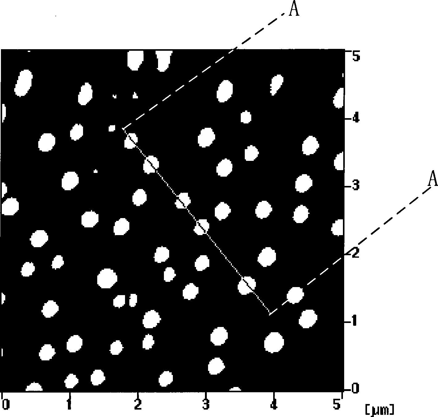
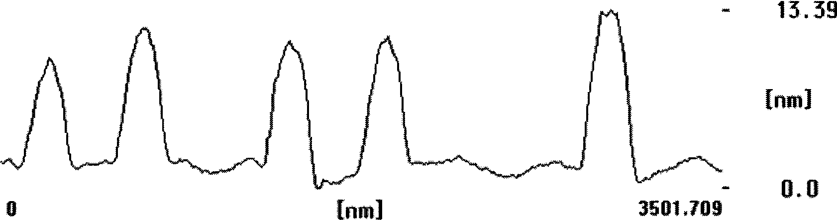
[0030] A physical vapor transport method is used to grow a millimeter-sized naphthacene single crystal under the background of an inert atmosphere at normal pressure. In a common high vacuum evaporation device, adjust the vacuum degree to 10 -3 Pa, using rubrene powder as the raw material, naphthacene single crystal as the substrate, and controlling the evaporation time to 4 minutes under the evaporation rate of 0.1nm / min. The surface of the film was tested by atomic force microscopy, and the morphology of rubrene micro-nanowires was determined by Figure 1a and Figure 1b It can be seen that the rubrene micro-nano wire is in the shape of a cone, with a diameter of about 300 nm at the bottom and a height of about 10 nm.

Embodiment 2

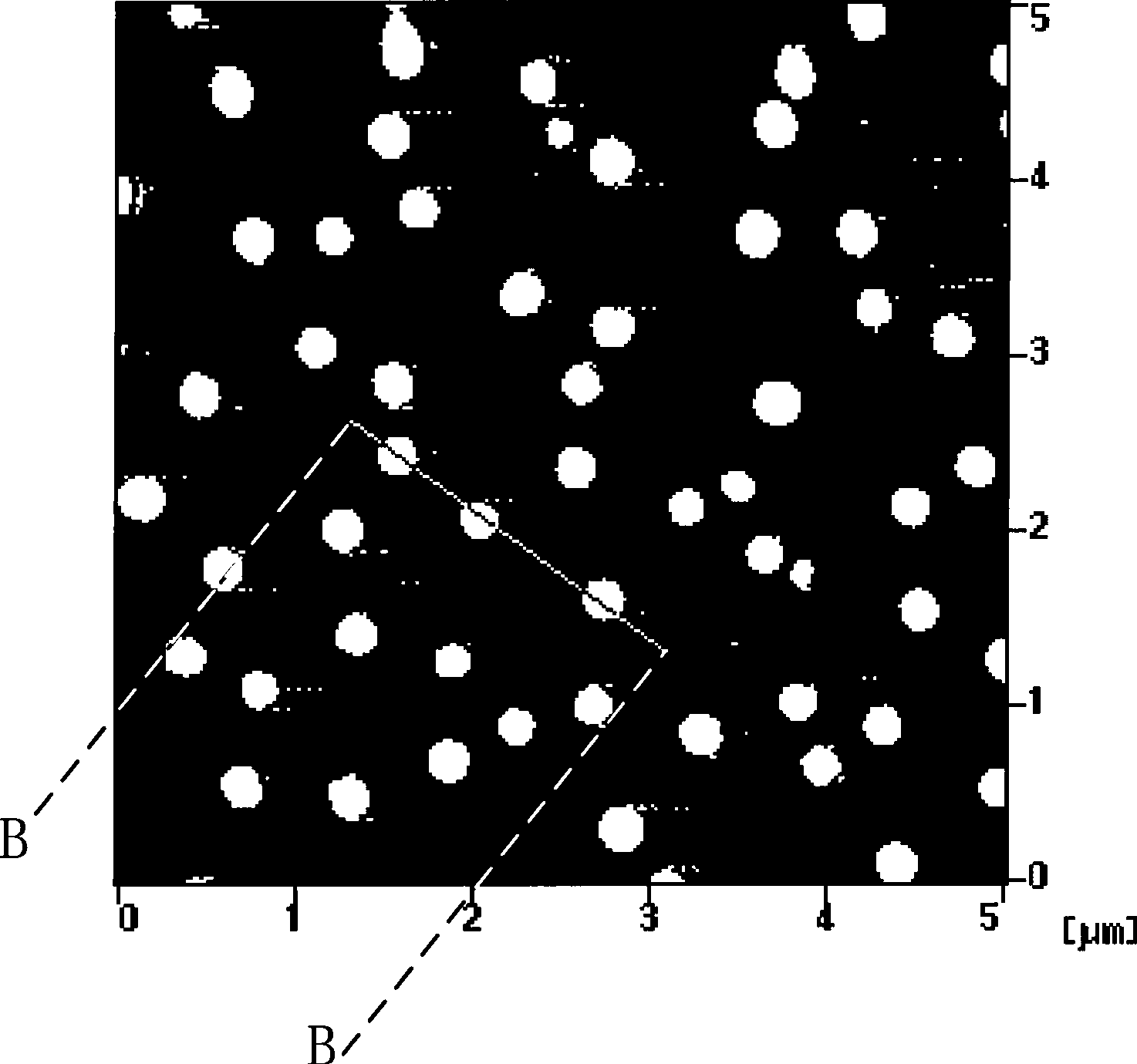
[0032] A physical vapor transport method is used to grow a millimeter-sized naphthacene single crystal under the background of an inert atmosphere at normal pressure. In a common high vacuum evaporation device, adjust the vacuum degree to 10 -3 Pa, using rubrene powder as the raw material, naphthacene single crystal as the substrate, and controlling the evaporation time to 8 minutes under the evaporation rate of 0.2nm / min. The surface of the film was tested by atomic force microscopy, and the morphology of rubrene micro-nanowires was determined by Figure 2a and Figure 2b It can be seen that the rubrene micro-nanowire is in the shape of a cone with a diameter of about 300 nm at the bottom and a height of about 20 nm.


PUM

PropertyMeasurementUnit
diameteraaaaaaaaaa
diameteraaaaaaaaaa
heightaaaaaaaaaa

Abstract

The invention discloses method of preparing rubrene micro-nanowire of organic semiconductor materials, and the method is characterized by using rubrene as a raw material for vapor deposition, using naphthacene single crystal growing through clean slices of silicon or physics gas-phase transmission method as the substrate, adopting a vacuum vapor deposition method, and under a condition of controlling the deposition rate and the deposition time, forming rubrene micro-nanowire with a standard size through deposition on the substrate of the semiconductor.According to the invention, because of adopting a vacuum vapor deposition method capable of controlling the deposition rate and deposition time accurately, the size of the rubrene micro-nanowire can be controlled accurately and simultaneously the preparation technique can also be simplified.

Description

technical field [0001] The invention relates to an organic semiconductor material rubrene, in particular to a controllable preparation method of the organic semiconductor material rubrene micro-nano wire. Background technique [0002] The rubrene material is an organic semiconductor that has been studied and applied more in recent years. In addition to its application in organic transistors, it has also played an unexpected and outstanding effect in OLEDs and solar cells. Since 2004, Sundar et al published the research results of rubrene single crystal transistors in the journal "Science" and showed that rubrene has the highest mobility in all organic materials (V.C.Sundar, et al, Science, 2004 , 303:1644), rubrene materials have received widespread attention, and more and more intelligent minds have begun to invest in research in this area. [0003] In 2006, Zhenan Bao et al. of Stanford University in the United States prepared rubrene micro-nano materials by combining phy...

Claims


Application Information

Patent Timeline
Patent Type & Authority Applications(China)
IPC IPC(8): C23C14/06C23C14/04C23C14/26H01L51/00
Inventor 曾雄辉徐科张锦平张露黄凯
Owner SUZHOU INST OF NANO TECH & NANO BIONICS CHINESE ACEDEMY OF SCI
Why Eureka
Try Eureka