Back contact type solar cell and manufacturing process thereof
A solar cell, back-contact technology, applied in circuits, photovoltaic power generation, electrical components, etc., can solve the problems of difficulty in large-scale industrialization and increase in process costs, and achieve the effect of reducing production costs and costs.
- Summary
- Abstract
- Description
- Claims
- Application Information
AI Technical Summary
Problems solved by technology
Method used
Image

Examples
Embodiment 1
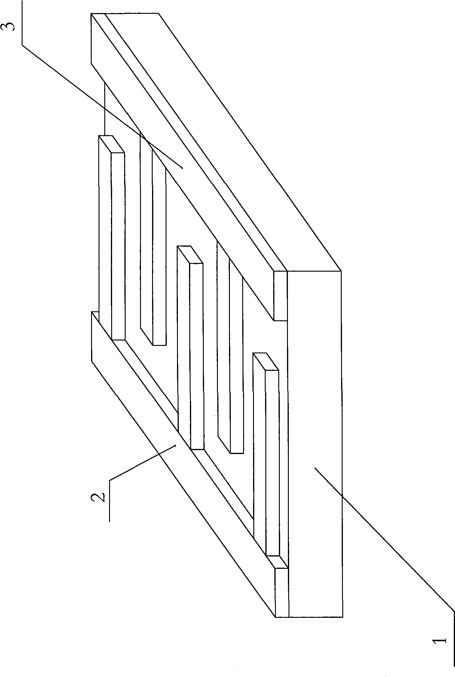
[0019] Using n-type (100) single crystal silicon with a sheet resistance of 100Ω / □ and a thickness of 180μm as the substrate material, the steps of cleaning, etching to remove the damaged layer, texturing and silicon nitride anti-reflection layer deposition are carried out by conventional processes. Two kinds of nickel slurries doped with 5% Al and 5% Sb were prepared respectively by ball milling technique. The two kinds of nickel pastes were printed on the back of the single crystal silicon substrate by two screen printing processes, dried and then sintered at a high temperature of 700°C. The patterns and printing positions of the two groups of doped nickel electrodes can just form interdigitated electrode pairs on the back of the silicon wafer. The fingers of the interdigitated electrodes have a width of 1 mm and a pitch of 0.3 mm, which are evenly distributed across the back of the silicon wafer. During high-temperature sintering of the electrode, Al in the Al-doped Ni pas...
Embodiment 2
[0021] Using n-type (100) single crystal silicon with a sheet resistance of 200 Ω / □ and a thickness of 180 μm as the substrate material, the damaged layer was removed, etched and textured, and cleaned using conventional processes. A 1% Al-doped Ni paste was prepared, and the Al-doped Ni paste was printed on the back of the silicon substrate by a screen printing process and dried. Prepare 1% Sb-doped nickel paste, print Sb-doped Ni paste on the back of silicon substrate by screen printing process, dry and sinter at 600°C to form interdigitated electrode pairs. The patterns and positions of the two metal electrodes are just enough to form interdigitated electrode pairs on the back of the silicon wafer. The interdigitated electrodes have a width of 1mm and a spacing of 0.3mm. Al in the Al-doped Ni slurry diffuses into the silicon in the slurry contact area, making this part of the silicon doped into p-type silicon and forming an ohmic contact with the metal electrode, while the S...
Embodiment 3
[0023] n-type polysilicon with a sheet resistance of 300Ω / □ and a thickness of 200μm is used as the substrate material. On the basis of conventional nickel slurry, 2% Al and 2% Sb doped Ni slurry were prepared respectively by ball milling mixing technology. After the polysilicon wafer has undergone damage layer removal, cleaning, texturing, and anti-reflection film deposition, two kinds of doped Ni pastes are printed on the back of the polysilicon substrate by a screen printing process and dried. The printed patterns and positions of the two metal pastes are just enough to form interdigitated electrode pairs on the back of the silicon wafer, followed by high-temperature sintering at 700°C to form interdigitated electrode pairs. The width of the interdigitated lines of the interdigitated electrodes is 2mm, and the pitch is 0.5mm. Al in the Al-doped Ni electrode diffuses into n-type silicon at high temperature, reverses to p-type, and forms an ohmic contact with the Al-doped Ni...
PUM
 Abstract
Description
Claims
Application Information
 - R&D
- Intellectual Property
- Life Sciences
- Materials
- Tech Scout
- Unparalleled Data Quality
- Higher Quality Content
- 60% Fewer Hallucinations
Browse by: Latest US Patents, China's latest patents, Technical Efficacy Thesaurus, Application Domain, Technology Topic, Popular Technical Reports.
© 2025 PatSnap. All rights reserved.Legal|Privacy policy|Modern Slavery Act Transparency Statement|Sitemap|About US| Contact US: help@patsnap.com