Optical thin-film structure used for laser crystal and preparation thereof

An optical thin film and laser crystal technology, applied in the field of semiconductor materials and optoelectronic materials, can solve the problems of interface stress mismatch, crystal structure and charge characteristics difference, thin film layering, etc., to improve performance and solve the problem of thin film damage.

Inactive Publication Date: 2009-07-08
SHANGHAI INST OF CERAMIC CHEM & TECH CHINESE ACAD OF SCI
View PDF0 Cites 10 Cited by
  • Summary
  • Abstract
  • Description
  • Claims
  • Application Information

AI Technical Summary

Problems solved by technology

Usually, the crystal structure and charge characteristics between the two are very different, and there is

Method used


Image

  • Optical thin-film structure used for laser crystal and preparation thereof

Examples


Embodiment 1

[0031] Example 1 The detailed preparation of the TiN buffer layer film is as follows:

[0032] 1 Raw material preparation. The raw materials used in this experiment to prepare TiN thin films are high-purity (4N) special particles for electron beam thermal evaporation.

[0033] 2 Substrate preparation. In this embodiment, ordinary optical K9 glass is selected as the substrate. First, put the substrate in NaOH solution for a quarter of an hour and repeat twice, then in absolute ethanol for a quarter of an hour, repeat twice, and finally in deionized water for a quarter of an hour. Then place the processed substrate in a vacuum oven for later use.

[0034] 3 Film growth. Divided into the following steps:

[0035] (1) The prepared electron beam thermal evaporation special 4N grade TiN particles and SiO 2 The dielectric film material and the cleaned K9 substrate are placed in a vacuum chamber, and the distance from the target to the substrate is adjusted to 50cm;

[0036] (2...

specific Embodiment

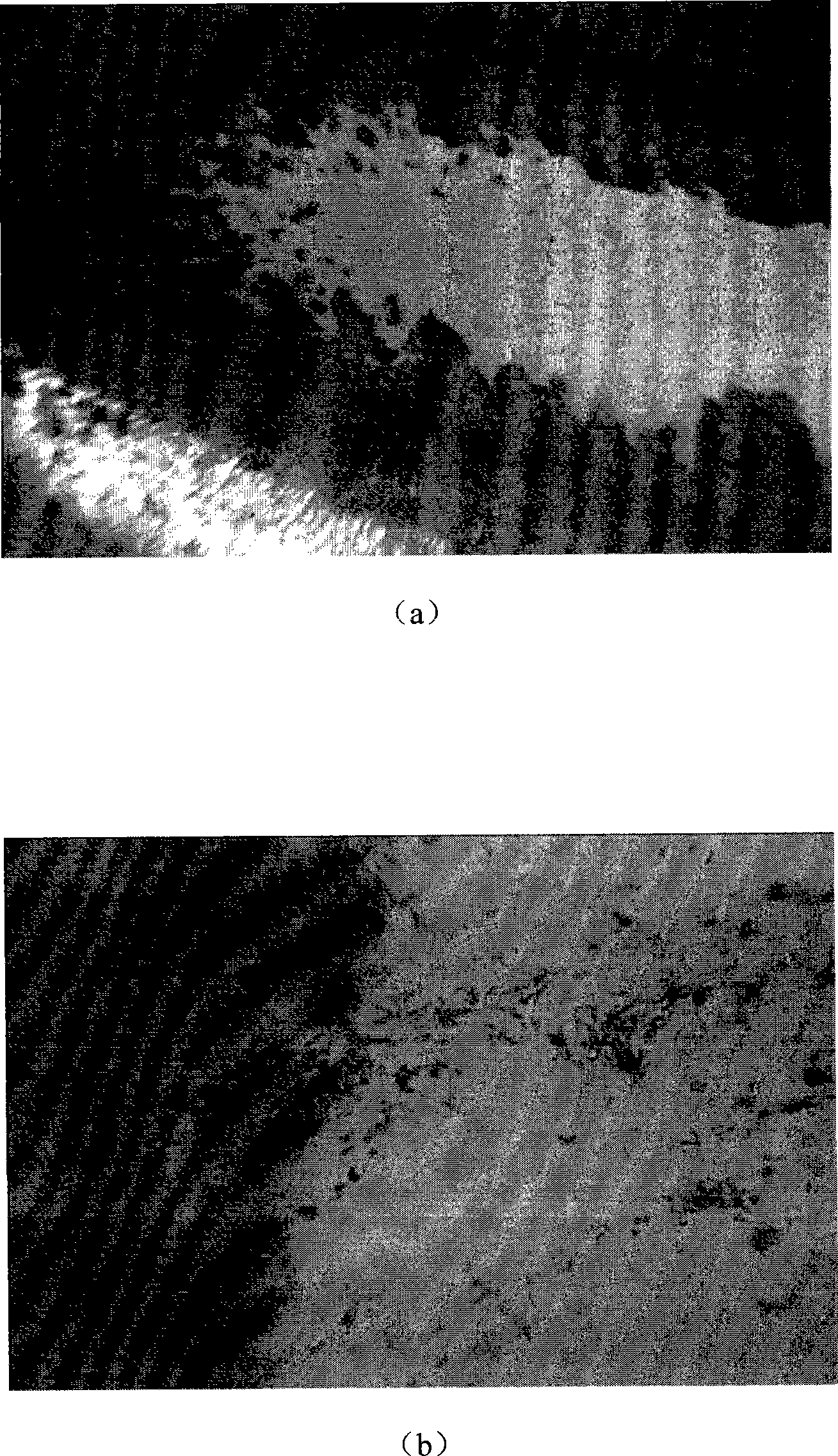
[0054] Concrete embodiment compares with comparative example anti-laser damage threshold test:


PUM

PropertyMeasurementUnit
Thicknessaaaaaaaaaa

Abstract

The invention relates to an optical thin film structure used for laser crystals, and a preparation method thereof. The invention is characterized in that a hard film buffer layer is added between the conventional complex film systems of media/metal used for laser crystals, plays a role in increasing the binding force of the media-metal complex film systems and improving the anti-laser radiation injury threshold of the complex film systems, and meets the development requirements of a high-power laser. The film of the buffer layer is prepared through the thermal evaporation of electron beams. During the growth process, TiN grains and a cleaned supporting base are arranged in a vacuum growth cabinet; the growth cabinet is vacuumized; electron beams are used for irradiating the TiN grains; a given amount of nitrogen or nitrogen ions is introduced into the vacuum cabinet; and the film of the TiN buffer layer is deposited on the supporting base. The TiN buffer layer can significantly improve the binding force of the complex film systems and the anti-laser radiator injury threshold. The optical thin film structure is very theoretically and practically significant for the high-power lasers developing quickly.

Description

technical field [0001] The present invention relates to an optical thin film structure for laser crystals and a preparation method thereof, more precisely relates to a buffer layer technology for a dielectric / metal composite film system of laser crystals, which is a buffer layer technology using titanium nitride thin films Layer to improve the bonding force of the dielectric / metal film system and the threshold value of anti-laser damage, the preparation method uses the electron beam vacuum deposition technology. The invention belongs to the fields of semiconductor materials and photoelectric materials. Background technique [0002] As an important optoelectronic device, laser is the basis of various photonic information or energy systems, and is also the core device of active optoelectronic weapons. It has been widely used in optical communication, optical information processing, laser processing, medicine and Military science and many other fields. Since the advent of the...

Claims


Application Information

Patent Timeline
IPC IPC(8): H01S3/042H01S3/16H01S3/0941
Inventor 李效民何西亮吴洁华宋力昕高相东
Owner SHANGHAI INST OF CERAMIC CHEM & TECH CHINESE ACAD OF SCI
Why Eureka
Try Eureka