Process for treating silicon through-hole interconnection construction

A process method and interconnection structure technology, which is applied in the manufacture of electrical components, circuits, semiconductors/solid-state devices, etc., can solve problems such as long working hours, increased costs, and overruns, so as to alleviate thermal mismatch, reduce parasitic capacitance, and reduce heat dissipation. The effect of mechanical stress

Active Publication Date: 2010-10-13
HUAZHONG UNIV OF SCI & TECH
View PDF0 Cites 0 Cited by
  • Summary
  • Abstract
  • Description
  • Claims
  • Application Information

AI Technical Summary

Problems solved by technology

[0005] This process flow can effectively realize high-density three-dimensional through-hole interconnection, but there are the following problems: (1) there is only a very thin insulating layer (usually silicon dioxide) between the silicon substrate and the copper structure layer , which leads to the formation of high capacitance between TSV interconnects, sometimes even exceeding the capacitance of standard wire-bonded interconnects; (2) fairly thick copper structures are filled in silicon holes
Due to the large thermal mismatch between silicon and copper, this will cause significant thermomechanical stress during thermal cycling; (3) the method of fully filling silicon holes with electroplated copper requires a long man-hour, which increases the process method cost

Method used


Image

  • Process for treating silicon through-hole interconnection construction
  • Process for treating silicon through-hole interconnection construction
  • Process for treating silicon through-hole interconnection construction

Examples


Embodiment Construction

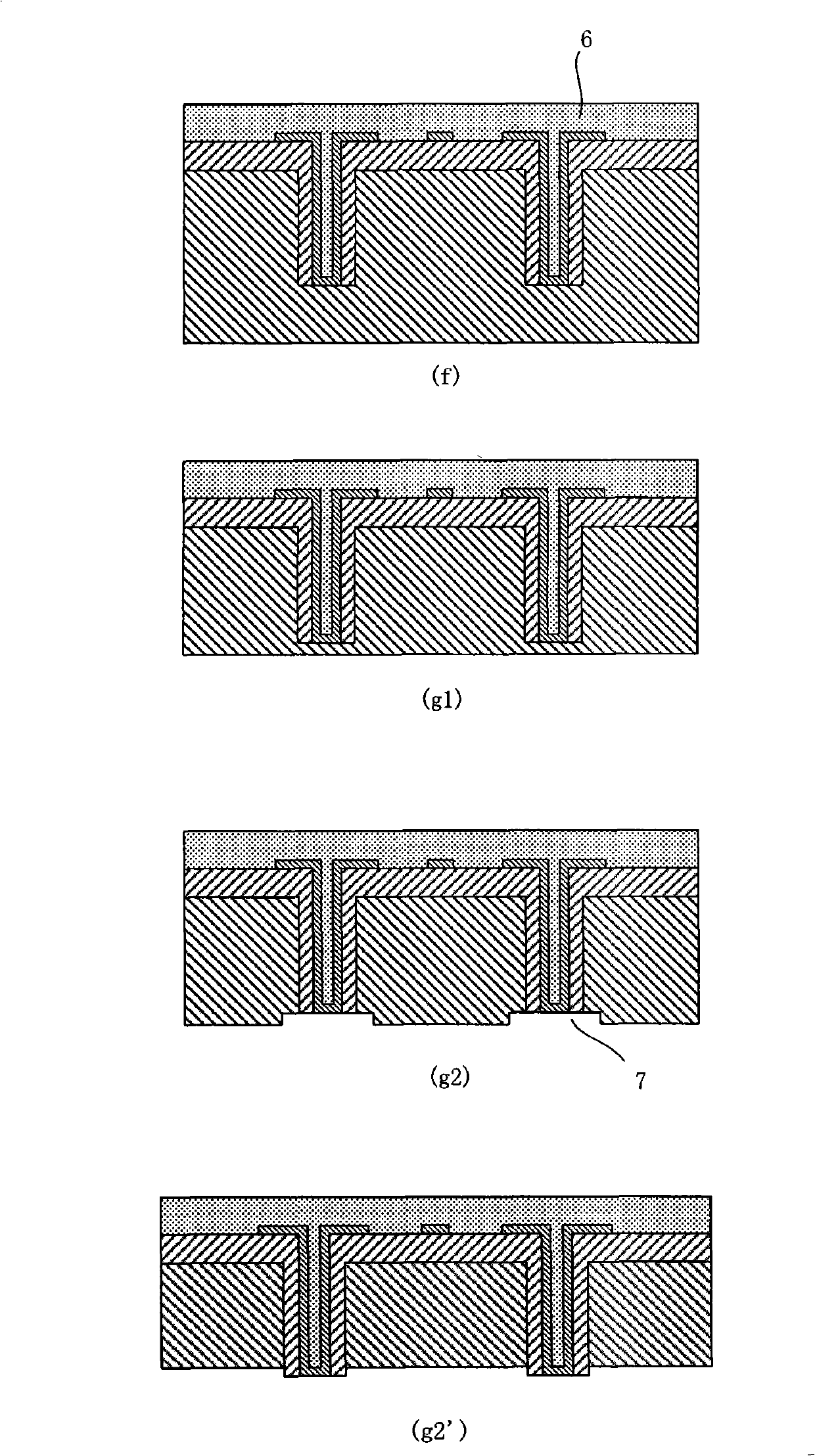
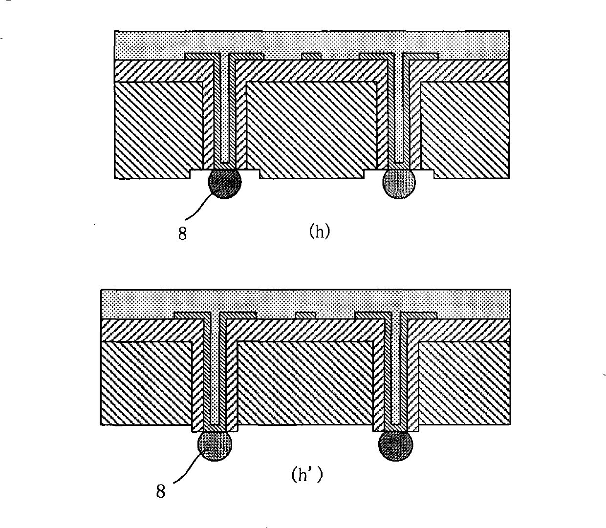
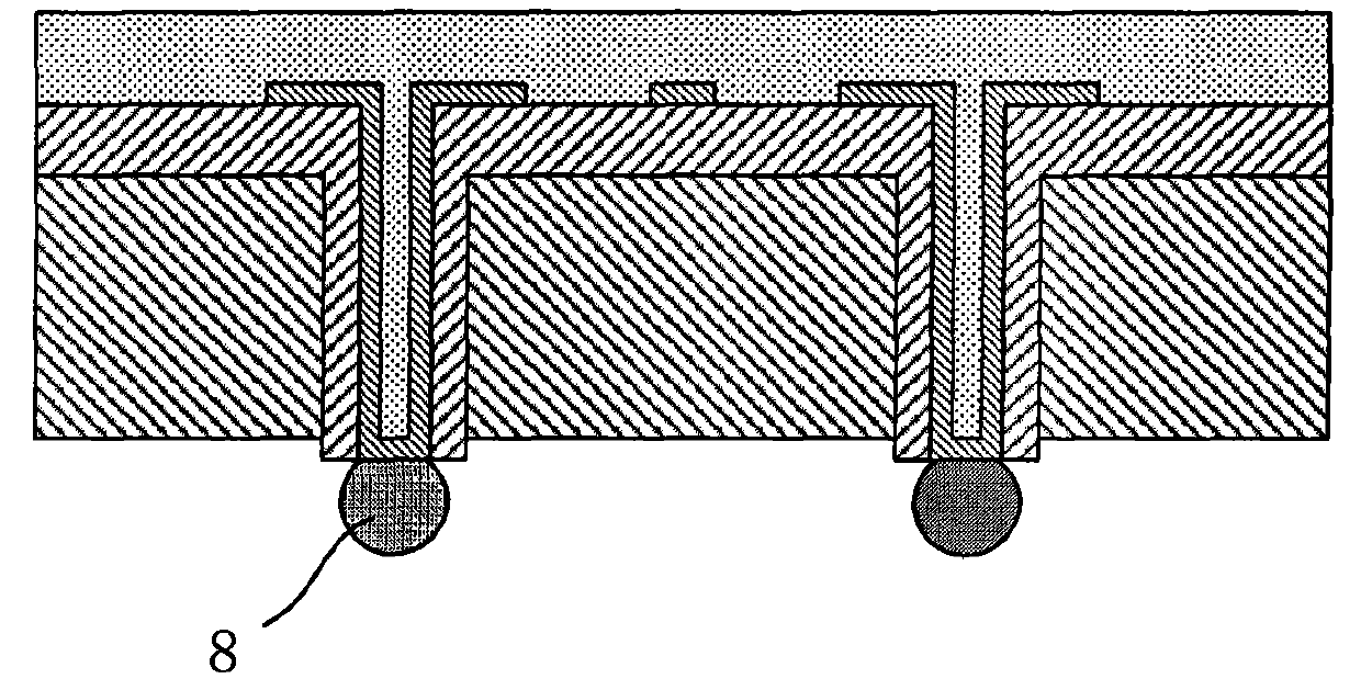
[0018] The specific implementation of the process method provided by the present invention will be further described in detail below in conjunction with the accompanying drawings and examples. The inventive method comprises:

[0019] (a) Provide a substrate 1 such as figure 1 (a) shows. The substrate can be a piece of unprocessed or processed wafer (such as silicon wafer or silicon device wafer), or it can be a microelectronic device. The thickness of the substrate is 10-500 microns.

[0020] (b) dry etching the above substrate 1 to form at least one blind hole 2 , and the aspect ratio of the blind hole 2 is 5:1-20:1. The blind holes 2 can have different shapes and sizes. Etching can use existing technology. Such as reflective ion etching-inductively coupled plasma technology (RIE-ICP) or deep reflected ion etching-inductively coupled plasma technology (DRIE-ICP). The width of the blind hole 2 is usually 20-100 microns, preferably 25 microns, and is most preferably cylind...


PUM

PropertyMeasurementUnit
thicknessaaaaaaaaaa
thicknessaaaaaaaaaa
thicknessaaaaaaaaaa

Abstract

The invention discloses a through wafer interconnect structure processing method comprising: 1. etching a blind hole on a substrate; 2. etching a pattern dielectric substance layer on the substrate; 3. etching the pattern dielectric substance layer and the dielectric material at the bottom of the blind hole, keeping the dielectric material of a blind hole side wall; forming a dielectric substancehole on the substrate; 4. depositing a layer of conductive material on the dielectric substance hole and forming a conductive hole; 5. re-depositing a layer of pattern dielectric substance on the conductive layer and filling the conductive hole; 6. etching the back side of the plate to expose the conductive layer and forming a solder micro-convex point on the conductive layer, wherein the patterndielectric substance material is preferable poly-p-xylene. The invention simplifies the process steps, reduces the process time and the cost; depresses a parasitic capacitance by using two layers of the pattern dielectric substance layers, improves a interconnect electrical behavior, suits for the high speed and RF three-dimensional interconnection structure; releases the thermal mismatch betweenthe conductive material and the silicon and greatly reduces the thermal mechanical stress.

Description

technical field [0001] The invention belongs to an electrical interconnection processing technology in the field of very large-scale integrated circuit manufacturing, and is particularly suitable for processing system-in-package (SiP), system-on-chip (SoC) and through-silicon via (TSV) interconnection structures in the form of three-dimensional stacking. technical background [0002] In the past forty years, the research, development and production of microelectronic components have been carried out in the direction predicted by Moore's law. In 2008, Intel and several other companies have begun to use 45 to 50 nanometer processing technology in the mass production of memory chips. According to this development trend, by 2012 at the latest, in order to further improve the integration of chips, 32 or even 22 nanometer processing technology will be required. However, the processing technology of 32 or 22 nanometers not only encounters the limitations of lithography equipment a...

Claims


Application Information

Patent Timeline
Patent Type & Authority Patents(China)
IPC IPC(8): H01L21/768
CPCH01L21/76898
Inventor 刘胜高鸣源胡程志吴一明
Owner HUAZHONG UNIV OF SCI & TECH
Why Eureka
Try Eureka