Gallium nitride-based high electron mobility transistor and preparation method thereof

A high electron mobility, gallium nitride-based technology, applied in the field of gallium nitride-based high electron mobility transistors and their preparation, can solve the problem of limited improvement in the quality of gallium nitride thin film crystals, affecting the high electron mobility of gallium nitride-based The performance of high-speed transistors can be solved, so as to alleviate the accumulation of dislocations and stress, reduce defects and dislocations, and improve the crystal quality.

Active Publication Date: 2022-07-15
JIANGXI ZHAO CHI SEMICON CO LTD
View PDF5 Cites 0 Cited by
  • Summary
  • Abstract
  • Description
  • Claims
  • Application Information

AI Technical Summary

Problems solved by technology

[0005] Aiming at the deficiencies of the prior art, the object of the present invention is to provide a gallium nitride-based high electron mobility transistor and its preparation method, aiming at solving the problem of conventional buffer layers between the silicon substrate and the gallium nitride thin film in the prior art. , GaN thin-film crystal quality improvement is limited, there are a large number of dislocations and defects, technical problems that affect the performance of GaN-based high electron mobility transistors

Method used


Image

  • Gallium nitride-based high electron mobility transistor and preparation method thereof
  • Gallium nitride-based high electron mobility transistor and preparation method thereof
  • Gallium nitride-based high electron mobility transistor and preparation method thereof

Examples


Embodiment 1

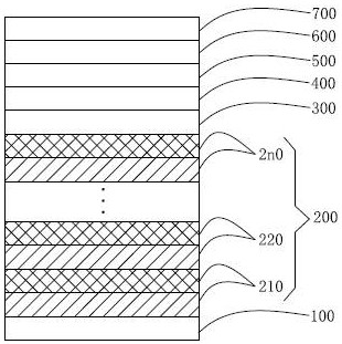
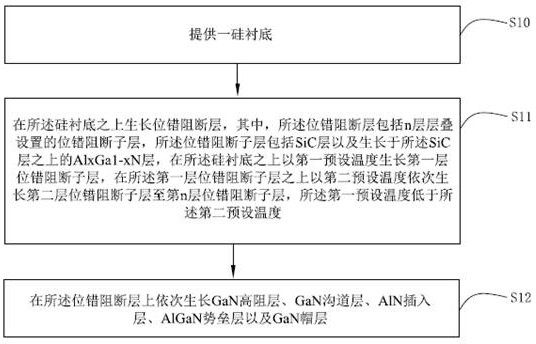
[0031] see figure 1 , shows a GaN-based high electron mobility transistor provided by the first embodiment of the present invention, the GaN-based high electron mobility transistor includes a silicon substrate 100; wherein, a silicon material is used as the substrate, and the It has the advantages of good thermal conductivity, large-scale epitaxial growth, high crystal quality, easy integration and low price, and has great market competitiveness.

[0032] The dislocation blocking layer 200 , the GaN high resistance layer 300 , the GaN channel layer 400 , the AlN insertion layer 500 , the AlGaN barrier layer 600 and the GaN cap layer 700 are sequentially stacked on the silicon substrate 100 . Among them, the dislocation blocking layer 200 is used to slow down the lattice mismatch and thermal mismatch between the silicon substrate 100 and the gallium nitride film, improve the crystal quality of the gallium nitride film, and improve the high electron mobility of the gallium nitri...

Embodiment 2

[0051] A second embodiment of the present invention provides a GaN-based high electron mobility transistor, the GaN-based high electron mobility transistor in this embodiment and the GaN-based high electron mobility transistor in the first embodiment The difference is:

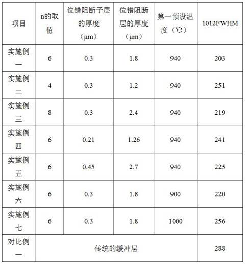
[0052] The dislocation blocking layer includes 4 dislocation blocking sub-layers stacked in layers, other conditions are the same, Al x Ga 1-x The composition ratio x of Al in the N layer is 0.15, and the thickness of the SiC layer is the same as that of Al. x Ga 1-x The thickness ratio of the N layer is 1:2, the thickness of the dislocation blocking sublayer is 0.3 μm, and the first preset temperature is 940°C.

Embodiment 3

[0054] A third embodiment of the present invention provides a GaN-based high electron mobility transistor, the GaN-based high electron mobility transistor in this embodiment and the GaN-based high electron mobility transistor in the first embodiment The difference is:

[0055] The dislocation blocking layer includes 8 dislocation blocking sub-layers arranged by stacking, other conditions are the same, Al x Ga 1-x The composition ratio x of Al in the N layer is 0.15, and the thickness of the SiC layer is the same as that of Al. x Ga 1-x The thickness ratio of the N layer is 1:2, the thickness of the dislocation blocking sublayer is 0.3 μm, and the first preset temperature is 940°C.


PUM

PropertyMeasurementUnit
thicknessaaaaaaaaaa
thicknessaaaaaaaaaa
thicknessaaaaaaaaaa

Abstract

The invention discloses a gallium nitride-based high-electron-mobility transistor and a preparation method thereof, and the gallium nitride-based high-electron-mobility transistor comprises a silicon substrate, and also comprises a dislocation blocking layer, a GaN high-resistance layer, a GaN channel layer, an AlN insertion layer, an AlGaN barrier layer and a GaN cap layer which are sequentially stacked on the silicon substrate. Wherein the dislocation blocking layer comprises n layers of dislocation blocking sub-layers which are arranged in a stacked mode, and each dislocation blocking sub-layer comprises a SiC layer and an Al < x > Ga < 1-x > N layer arranged on the SiC layer. The silicon substrate and the gallium nitride thin film are provided with traditional buffer layers in the prior art, the crystal quality improvement amplitude of the gallium nitride thin film is limited, and a large number of dislocation and defects exist; and the performance of the gallium nitride-based high-electron-mobility transistor is influenced.

Description

technical field [0001] The invention relates to the technical field of semiconductors, in particular to a gallium nitride-based high electron mobility transistor and a preparation method thereof. Background technique [0002] With the continuous development of semiconductor technology, high electron mobility transistor (HEMT) is a type of field effect transistor, which uses two materials with different energy gaps to form a heterojunction to provide a channel for carriers , and Gallium Nitride (GaN)-based high electron mobility transistors have attracted a lot of attention due to their good high-frequency characteristics. Therefore, GaN-based high electron mobility transistors can work at very high frequencies and are widely used in In the field of mobile phones, satellite TV and radar. [0003] At present, the more common GaN-based high electron mobility transistors usually use single crystal silicon as the substrate material for growing gallium nitride. Due to the large s...

Claims


Application Information

Patent Timeline
Patent Type & Authority Applications(China)
IPC IPC(8): H01L29/15H01L29/778H01L21/335
CPCH01L29/151H01L29/158H01L29/7787H01L29/66462
Inventor 侯合林谢志文张铭信陈铭胜
Owner JIANGXI ZHAO CHI SEMICON CO LTD
Why Eureka
Try Eureka