Co-Ga co-blended ZnO based diluted semi-conductor thin-film and manufacturing method thereof

A dilute magnetic semiconductor and thin-film technology, which is used in the manufacture of semiconductor/solid-state devices, the manufacture/processing of electromagnetic devices, and the selection of materials, etc., can solve problems with room temperature ferromagnetism, high carrier concentration, etc. Mature craftsmanship and easy-to-achieve effects

Inactive Publication Date: 2009-07-15
ZHEJIANG UNIV
View PDF0 Cites 17 Cited by
  • Summary
  • Abstract
  • Description
  • Claims
  • Application Information

AI Technical Summary

Problems solved by technology

[0003] The research on ZnO-based DMS materials is still in the basic research stage. If it is to be applied, t

Method used


Image

  • Co-Ga co-blended ZnO based diluted semi-conductor thin-film and manufacturing method thereof
  • Co-Ga co-blended ZnO based diluted semi-conductor thin-film and manufacturing method thereof
  • Co-Ga co-blended ZnO based diluted semi-conductor thin-film and manufacturing method thereof

Examples


Embodiment 1

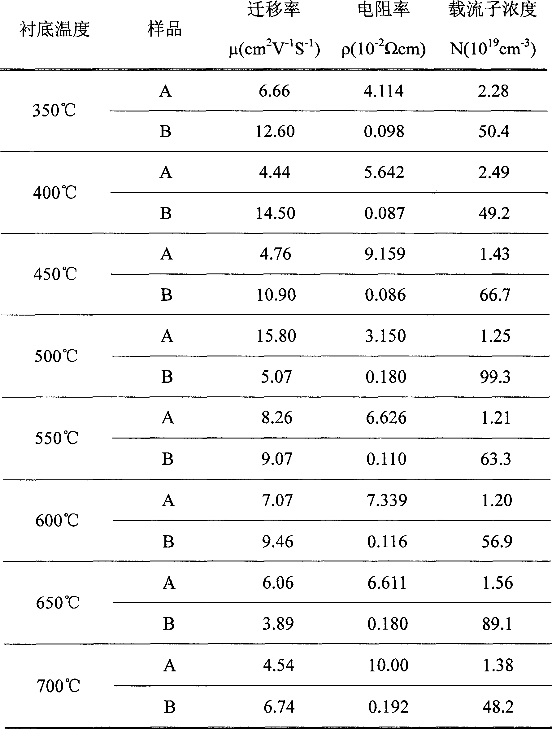
[0017] 1) Preparation of ceramic target. Weigh pure ZnO, Co 2 o 3 , Ga 2 o 3 powder, wherein the molar percentage of Co is 2%, the molar percentage of Ga is 3%, and the weighed ZnO, Co 2 o 3 , Ga 2 o 3 The powder was poured into a ball mill jar equipped with agate balls, and milled on a ball mill for 24 hours to make ZnO, Co 2 o 3 , Ga 2 o 3 The powder is well mixed and finely ground. Then the raw materials are separated and dried, added with a binder for grinding, and pressed into shape. Put the formed green body into the sintering furnace, first keep it warm at 800°C for 2 hours to volatilize the binder, then raise the temperature to 1250°C for 2 hours and sinter to obtain Zn(Co, Ga)O ceramic target.

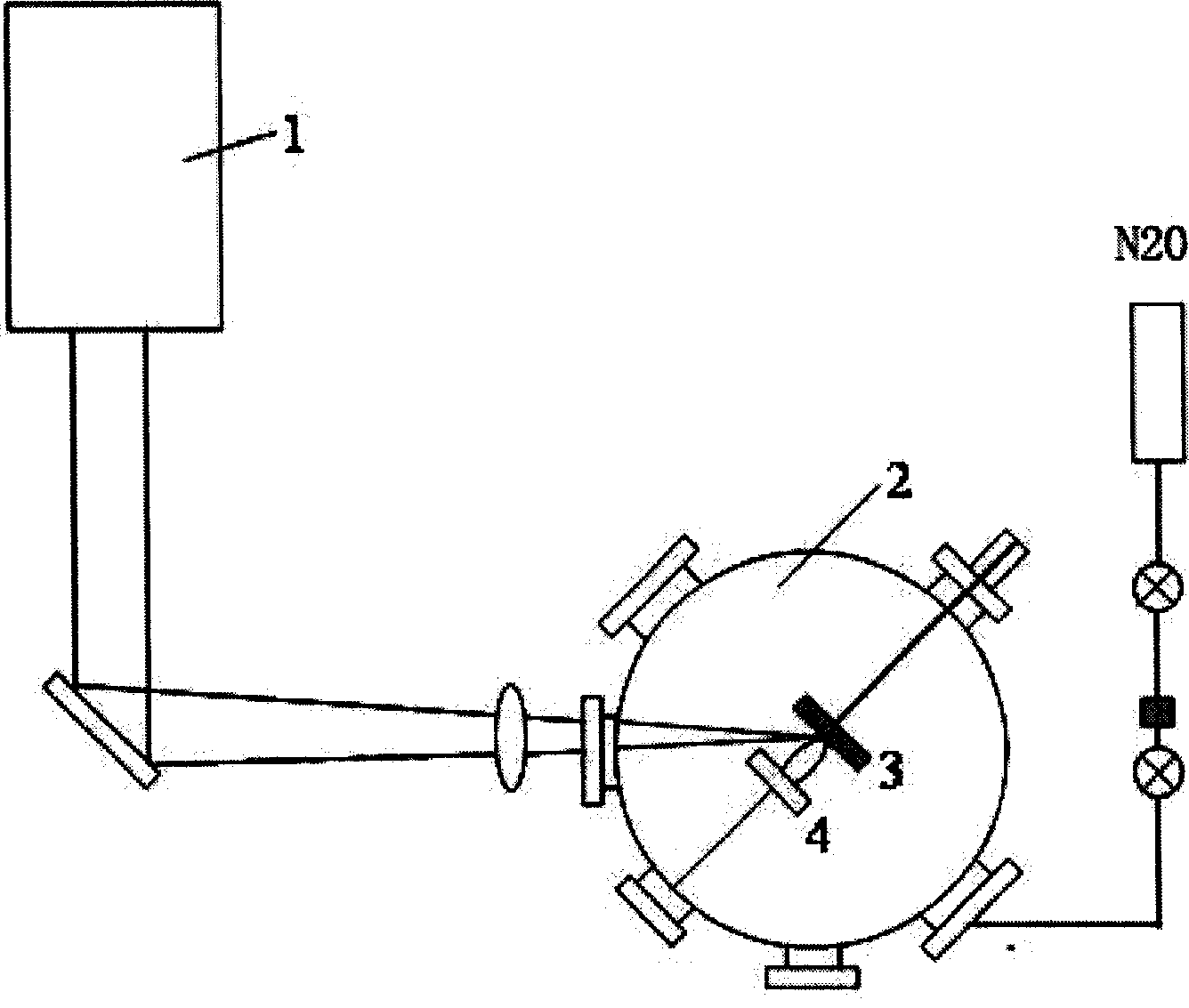
[0018] 2) Use a 2-inch quartz polished wafer as the substrate, clean the surface of the substrate and put it into the growth chamber of the pulsed laser deposition system. The vacuum degree of the growth chamber is evacuated to less than 8.0×10 -4 Pa, then heat th...

Embodiment 2

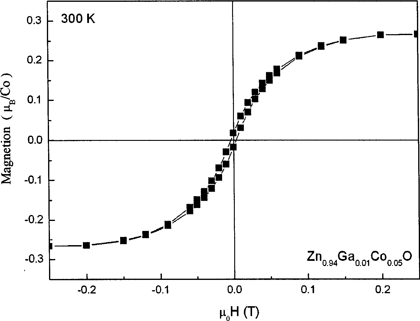
[0022] The target material preparation and film deposition process are the same as in Example 1, wherein the molar percentage of Co is 10%, and the molar percentage of Ga is 3%, and a Co-Ga co-doped ZnO dilute magnetic semiconductor film with high Carrier concentration and room temperature ferromagnetism.

Embodiment 3

[0024] The target preparation and film deposition process are the same as in Example 1, the difference is that the substrate is sapphire, and the substrate temperature rises to 700°C, and a Co-Ga co-doped ZnO dilute magnetic semiconductor film with high carrier concentration and Ferromagnetic at room temperature.


PUM


Abstract

The invention discloses a Co-Ga codoped Zno base diluted magnetic semiconductor film, wherein a Co molar content is more or equal than 2and less or equal to 10, a Ga molar content is more or equal to 1and less or equal to 3 The diluted magnetic semiconductor film is prepared by a pulsed laser deposition method and a pure ZnO, Co2O3, a Ga2O3 powder mixed sintered ceramic chip is employed as a target material. A substrate is placed in a growth chamber of a pulsed laser deposition device after cleaning the substrate, and the growth chamber is vacuumized to a background vacuum less than 8.0 *10 Pa. The mixture is grown under an O2 atmosphere with a pressure of 2-15Pa and a temperature of 350-700 DEG C. The preparation method of the invention is simple, an n type doping carrier concentration can reach 5.0*10-5.0*10 cm and simultaneously have a room temperature iron magnetic property.

Description

technical field [0001] The invention relates to a method for preparing a ZnO-based dilute magnetic semiconductor film with high carrier concentration n-type and room temperature ferromagnetic properties. Background technique [0002] Diluted Magnetic Semiconductors (DMS) is the introduction of magnetic ions into the semiconductor material by doping, so that the magnetic ions partially replace the non-magnetic cations in the semiconductor, forming a material with dual properties of electronic charge and spin. It can be used to prepare new devices integrating optical, electrical and magnetic functions, such as various ultra-low energy consumption and high-density information memories, logic devices and spin polarized light emitters. Diluted magnetic semiconductors are spin-polarized semiconductors. Usually, dilute magnetic semiconductors are prepared by doping a small amount of 3d transition group elements into semiconductor materials to produce ferromagnetism while maintainin...

Claims


Application Information

Patent Timeline
IPC IPC(8): H01L43/10H01L43/12H01L21/203H01L21/363C23C14/34
Inventor 叶志镇张利强张银珠吕建国何海平朱丽萍
Owner ZHEJIANG UNIV
Why Eureka
Try Eureka