Absolute pressure transducer chip based on surface micro-machining and its production method

A sensor chip, micromachining technology, applied in the process of producing decorative surface effects, chemical instruments and methods, fluid pressure measurement by changing ohmic resistance, etc., can solve the problem of high initial cost, device failure, leakage current Large and other problems, to achieve the effect of high sensitivity, good stability, and stable performance

Active Publication Date: 2009-07-22
SHANGHAI INST OF MICROSYSTEM & INFORMATION TECH CHINESE ACAD OF SCI
View PDF0 Cites 21 Cited by
  • Summary
  • Abstract
  • Description
  • Claims
  • Application Information

AI Technical Summary

Problems solved by technology

[0004] However, the fabrication of the absolute pressure sensor chip based on bulk micromachining has the following disadvantages: first: the pn junction is isolated between the resistance after power-on and the silicon substrate, and when the temperature of the device is above 100°C, the pn junction The leakage current is very large, which makes the device unable to work, so it cannot meet the use of stress test in medium and high temperature environment
Second: In order to obtain a vacuu

Method used


Image

  • Absolute pressure transducer chip based on surface micro-machining and its production method
  • Absolute pressure transducer chip based on surface micro-machining and its production method
  • Absolute pressure transducer chip based on surface micro-machining and its production method

Examples


Embodiment Construction

[0017] The substantive features and remarkable progress of the present invention will be further described below through specific implementation, but the present invention is by no means limited to the described embodiments.

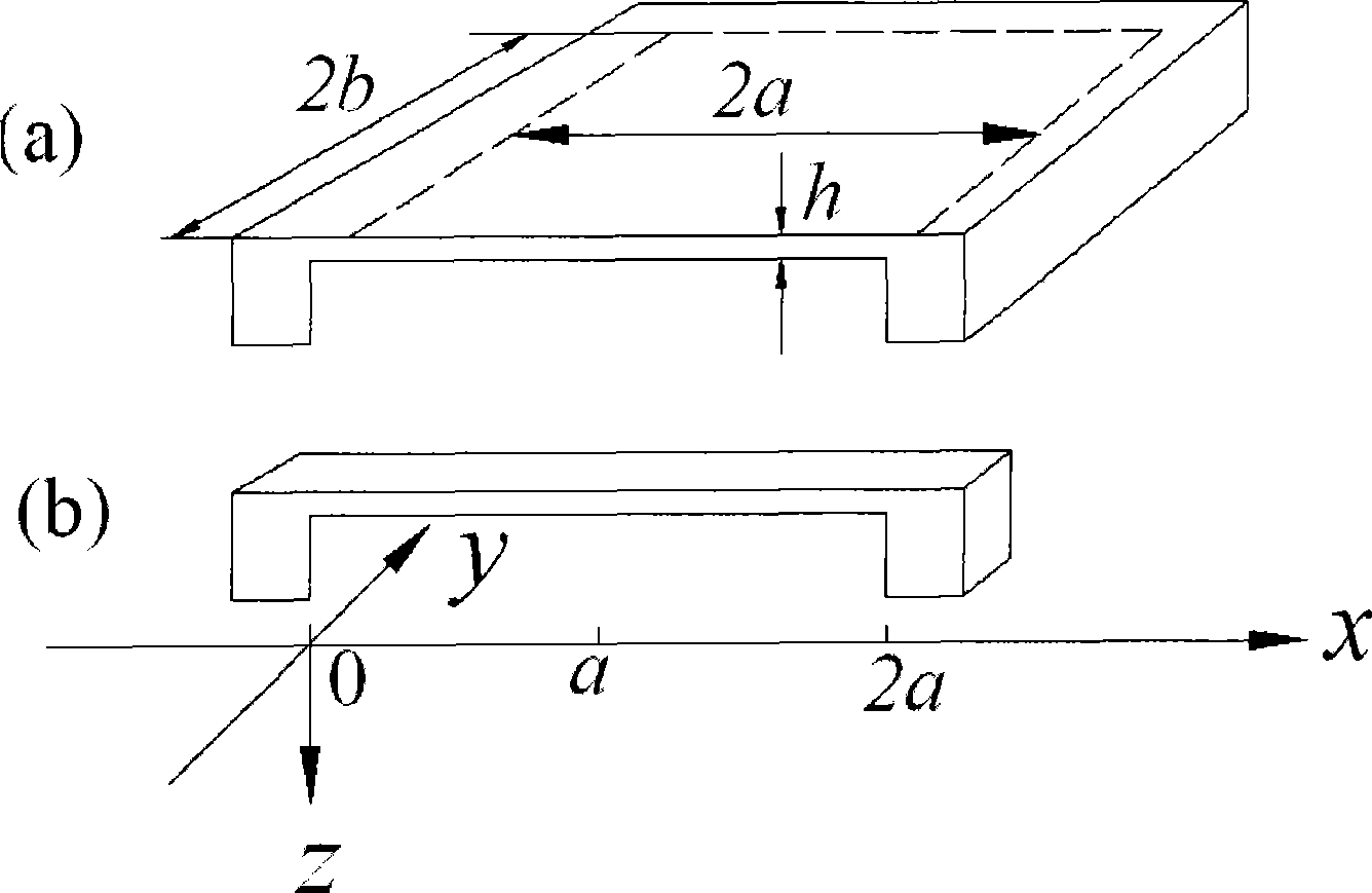
[0018] Absolute pressure sensor chip based on surface micromachining with a range of 450KPa and its manufacturing method: the thickness h of the designed LS SiN structure layer is 1.2 μm, the long side 2b of the long rectangular film region is 360 μm, and the short side 2a is 48 μm, as figure 1 (a) shown. The thickness of the polysilicon resistor is 0.4 μm, the resistance value is 5000 ohms, and the thickness of the sacrificial layer is 2 μm.

[0019] The specific implementation steps are:

[0020] 1. Build a sacrificial layer,

[0021] Such as Figure 5As shown in (a), since the surface microcomputer machining is only processed on one side, the initial silicon wafer can be a double-polished or single-polished silicon wafer, and there is no requiremen...


PUM


Abstract

The invention relates to an absolute pressure sensor chip based on surface micromachining and a manufacturing method. The manufacturing method is characterized by comprising the following steps: adopting a low-stress silicon nitride film as a core structural layer of the pressure sensor chip and using a polycrystalline silicon film to form a force-sensitive resistor track; designing a film area of the low-stress silicon nitride film into a long rectangle, fully utilizing longitudinal piezoresistive effect of the polycrystalline silicon resistor track according to the stress distribution of the film area, and making the most of a tensile stress area on the film to put part of a pair of resistor tracks on the external surface of the film and arrange another two resistor tracks on the central position of the film; and separately contacting a folded bent angle part of each resistor track with a hole depositing metal to conduct the bent angle part. By adopting surface micromachining technology compatible with IC technology, the method can manufacture the absolute pressure sensor chip with a measuring range of 1KPa-1MPa and with high sensitivity, good stability and high precision.

Description

technical field [0001] The present invention relates to providing an absolute pressure sensor chip based on surface micromachining and its manufacturing method, more precisely, providing a low-stress silicon nitride film as a structural layer, and a polysilicon film forming a force-sensitive resistor and adopting surface micromachining An absolute pressure sensor chip and a manufacturing method thereof belong to the technical field of silicon micromechanical sensors. Background technique [0002] The piezoresistive pressure sensor appeared in the 1960s. The subsequent development of micromachining technology made the sensitive components miniaturized, the sensor production was mass-produced, and the cost was reduced. It established a dominant position in the field of pressure measurement. Compared with the traditional Membrane potentiometer, force balance, variable inductance, variable capacitance, metal strain gauge and semiconductor strain gauge sensors are much more advan...

Claims


Application Information

Patent Timeline
IPC IPC(8): G01L1/18G01L9/06B81C5/00B81B7/02B81C1/00
Inventor 王权李昕欣鲍敏杭
Owner SHANGHAI INST OF MICROSYSTEM & INFORMATION TECH CHINESE ACAD OF SCI
Why Eureka
Try Eureka