Solution method preparation for metal photon crystal

A metal photonic crystal and solution method technology, applied in the field of nano-optoelectronic materials and devices, can solve the problems of limiting the wide application of metal photonic crystals, low preparation efficiency, and small preparation area, and achieve low cost, high preparation efficiency, and good repeatability Effect

Inactive Publication Date: 2011-06-29
BEIJING UNIV OF TECH
View PDF0 Cites 2 Cited by
  • Summary
  • Abstract
  • Description
  • Claims
  • Application Information

AI Technical Summary

Problems solved by technology

However, these preparation methods have disadvantages such as small preparation area (<200 μm), low efficiency, and high cost, which greatly limit the wide application of metal photonic crystals.
In recent years, interference lithography combined with dry etching technology is a new method for large-scale preparation of metal photonic crystals. However, this method still has problems such as high preparation cost and low preparation efficiency.

Method used


Image

  • Solution method preparation for metal photon crystal
  • Solution method preparation for metal photon crystal
  • Solution method preparation for metal photon crystal

Examples


Embodiment 1

[0029] Fabrication of waveguide-coupled one-dimensional nanowire gold photonic crystal structures

[0030] The photoresist used in this embodiment is positive photoresist S1805 produced by Germany ROHM & HAAS company; the substrate is a glass plate coated with a 200nm ITO waveguide layer.

[0031] 1) Spin-coat the photoresist S1805 on the surface of the ITO by spin-coating at a speed of 1500rpm to obtain a photoresist film with a thickness of 200nm;

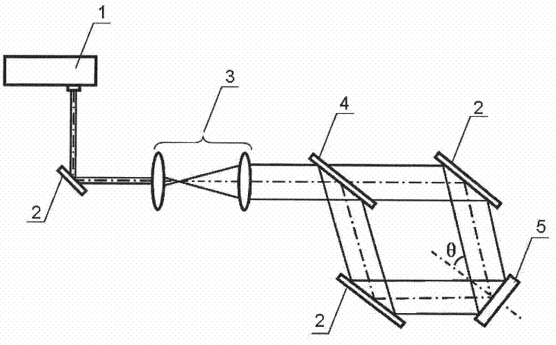
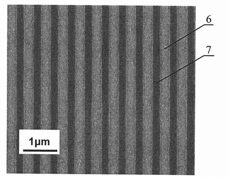
[0032] 2) Use such as figure 1 The optical path of the interference lithography is shown, wherein the θ angle in the interference optical path is 19.5 degrees, and the output power of the laser is 0.1mW. The sample is placed in figure 1 On the sample rack shown, expose for 3s, develop for 8s with developing solution, and obtain a one-dimensional photoresist nano-grating structure, such as figure 2 As shown, the period of the grating structure is 500nm;

[0033] 3) After preparing gold nanoparticles with a diameter of 2-7nm wi...

Embodiment 2

[0037] Preparation of two-dimensional nanopillar gold photonic crystal structure

[0038] The photoresist used in this embodiment is a negative photoresist ma-N405 produced by Microresist Company of Germany; the substrate is a glass sheet.

[0039] 1) The photoresist ma-N405 is spin-coated on the surface of the glass by the method of spin coating, and the rotation speed is 2000rpm to obtain a photoresist film with a thickness of 150nm;

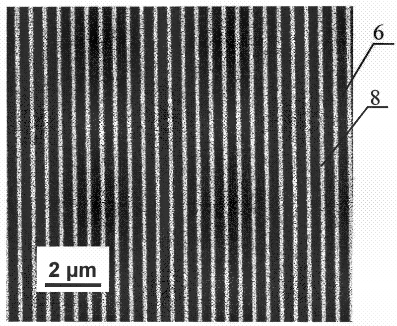
[0040] 2) Use such as figure 1 The optical path of the interference lithography shown, wherein, the θ angle in the interference optical path is 28 degrees, the light output power of the laser is 0.1mW, the sample is placed in figure 1 On the sample rack shown, expose for 2s, rotate the sample 90 degrees for secondary exposure, develop with developer for 4s, and obtain a two-dimensional photoresist nanohole grating structure, the period of the two-dimensional grating structure is 330nm;

[0041] 3) After preparing gold nanoparticles with a di...

Embodiment 3

[0045] Fabrication of Waveguide-Coupled Two-Dimensional Nanohole Gold Photonic Crystal Structures

[0046] The photoresist used in this embodiment is positive photoresist S1805 produced by Germany ROHM & HAAS company; the substrate is a glass plate coated with a 200nm ITO waveguide layer.

[0047] 1) Spin-coat the photoresist S1805 on the surface of the ITO by spin-coating at a speed of 4000rpm to obtain a photoresist film with a thickness of 50nm;

[0048] 2) Use such as figure 1 The optical path of the interference lithography shown, wherein, the θ angle in the interference optical path is 28 degrees, the light output power of the laser is 0.1mW, the sample is placed in figure 1 On the sample rack shown, expose for 2s, rotate the sample 90 degrees for secondary exposure, develop with developer for 4s, and obtain a two-dimensional photoresist nanopillar grating structure, the period of the two-dimensional grating structure is 330nm;

[0049] 3) After preparing gold nanopart...


PUM

PropertyMeasurementUnit
thicknessaaaaaaaaaa
thicknessaaaaaaaaaa

Abstract

The solution method for preparing metal photonic crystal belongs to the technical field of nano photoelectron materials and devices thereof. The existing method for preparing metal photonic crystal is faced with the problems such as high cost, low efficiency and small area of preparation, etc. In the invention, sequentially, optical resist is rotatably coated on a substrate; the interference photolithography is adopted to prepare one-dimensional or two-dimensional nano optical grating structures; metal nano particle sol is rotatably coated and goes through low temperature heat treatment, thusobtaining the metal photonic crystal. The invention has the advantages of low cost, high efficiency and preparation of the metal photonic crystal in a large acreage and the like.

Description

technical field [0001] The invention belongs to the technical field of nano-optoelectronic materials and devices, in particular to a method for preparing a one-dimensional / two-dimensional metal photonic crystal, in particular to a one-dimensional / two-dimensional metal photonic crystal with controllable preparation period and duty ratio combined with interference lithography and solution method Methods for metal photonic crystals. Background technique [0002] Periodically arranged metal nanowires, metal nanopillars or metal nanoholes are often called metal photonic crystals. Electromagnetic waves incident on metal photonic crystals will cause collective oscillation of electrons in the metal, resulting in localized surface plasmon resonance. It has important application prospects in fields such as cavities and biosensors. At present, a variety of methods have been applied to the preparation of one-dimensional / two-dimensional / three-dimensional metal photonic crystals, such a...

Claims


Application Information

Patent Timeline
Patent Type & Authority Patents(China)
IPC IPC(8): G03F7/00G02B6/122
Inventor 张新平刘红梅
Owner BEIJING UNIV OF TECH
Why Eureka
Try Eureka