N type SOI lateral double-diffused metal-oxide semiconductor transistor
An oxide semiconductor and lateral double-diffusion technology, which is applied in semiconductor devices, semiconductor/solid-state device manufacturing, electrical components, etc., can solve the problems of complex manufacturing process, reduce bonding strength, and unfavorable heat dissipation of devices, so as to avoid photolithography The effect of alignment problem, reduction of integral length, and reduction of process difficulty
- Summary
- Abstract
- Description
- Claims
- Application Information
AI Technical Summary
Problems solved by technology
Method used
Image

Examples
Embodiment Construction
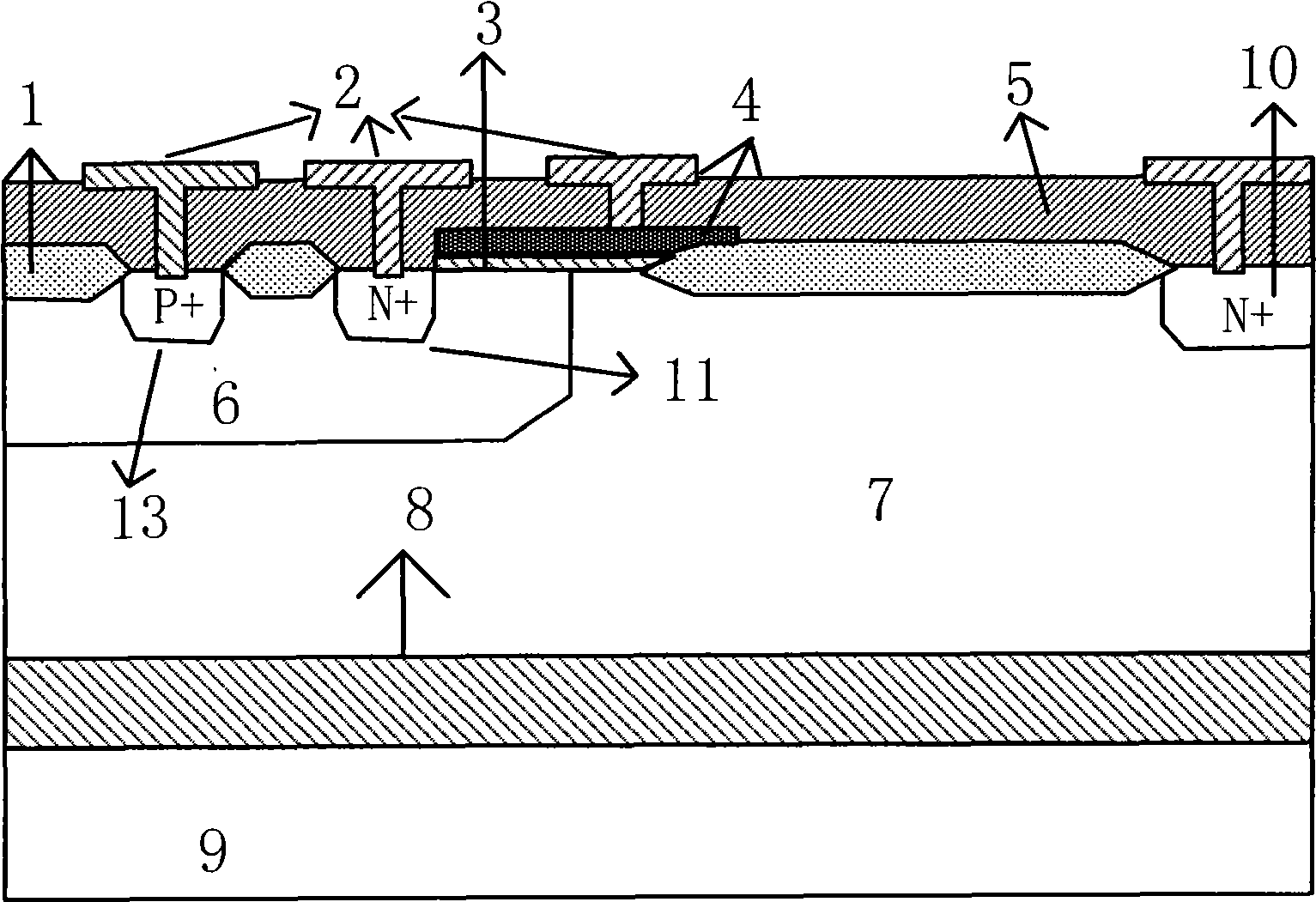
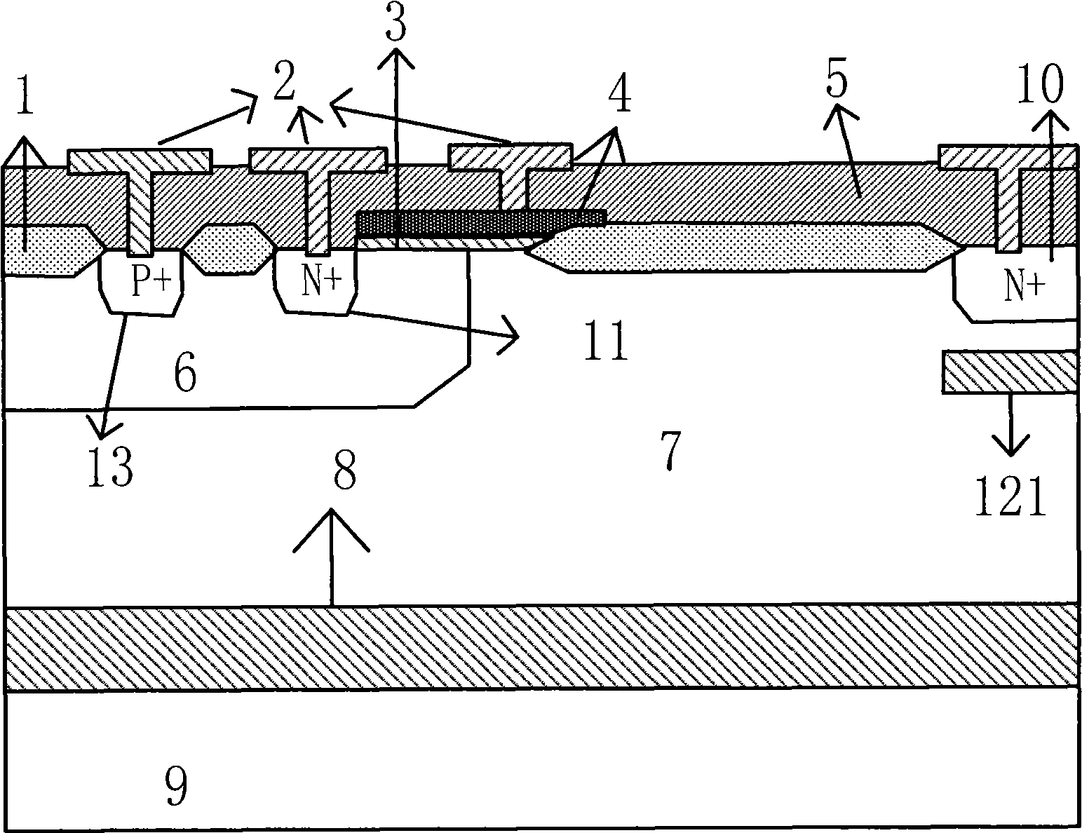
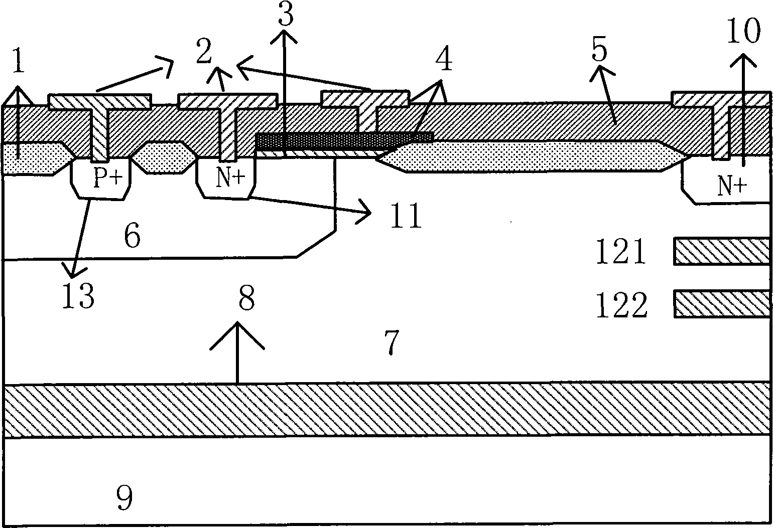
[0019] refer to figure 2 , an N-type silicon-on-insulator lateral double-diffused metal oxide semiconductor transistor, comprising: a semiconductor substrate 9, a buried oxide layer 8 is arranged on the semiconductor substrate 9, and an N-type doped layer is arranged on the buried oxide layer 8 Semiconductor region 7 is provided with P well 6 and N type drain region 10 on N type doped semiconductor region 7, is provided with N type source region 11 and P type contact region 13 on P well 6, on the surface of P well 6 A gate oxide layer 3 is provided and the gate oxide layer 3 extends from the P well 6 to the N-type doped semiconductor region 7, and the N-type source region 11 on the surface of the P well 6, the P-type contact region 13 and the area other than the gate oxide layer 3 A field oxide layer 1 is provided in the area other than the N-type drain region 10 on the surface of the N-type doped semiconductor region 7, and a polysilicon gate 4 is provided on the surface of ...
PUM
| Property | Measurement | Unit |
|---|---|---|
| Thickness | aaaaa | aaaaa |
Abstract
Description
Claims
Application Information