Lateral double-diffused metal-oxide-semiconductor transistor of silicon on N-type insulator
An oxide semiconductor and lateral double-diffusion technology, which is applied in the direction of semiconductor devices, electrical components, circuits, etc., can solve the problems of increased device on-resistance, increased device power consumption, unfavorable source region and middle region withstand voltage, etc., to reduce The effects of on-resistance, improvement of overall withstand voltage, and area reduction
- Summary
- Abstract
- Description
- Claims
- Application Information
AI Technical Summary
Problems solved by technology
Method used
Image

Examples
Embodiment Construction
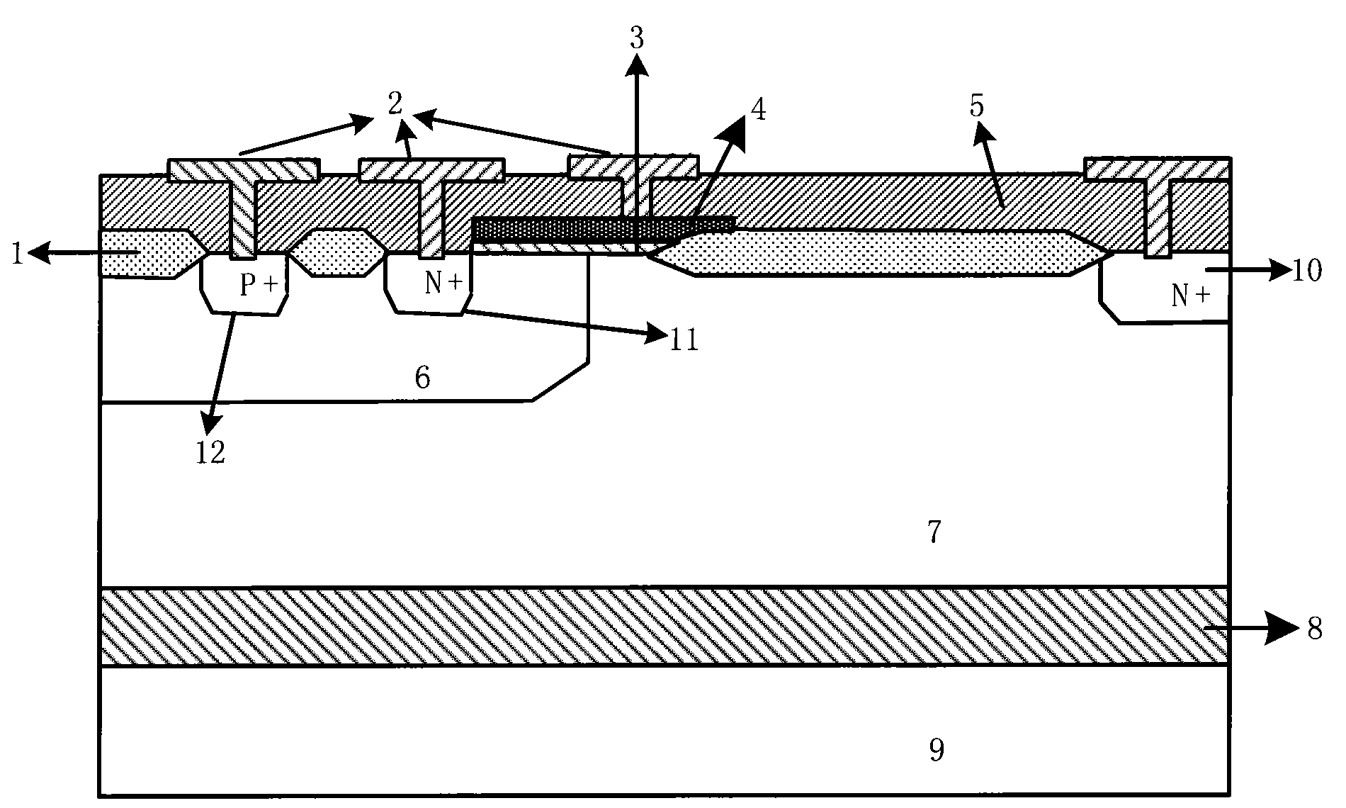
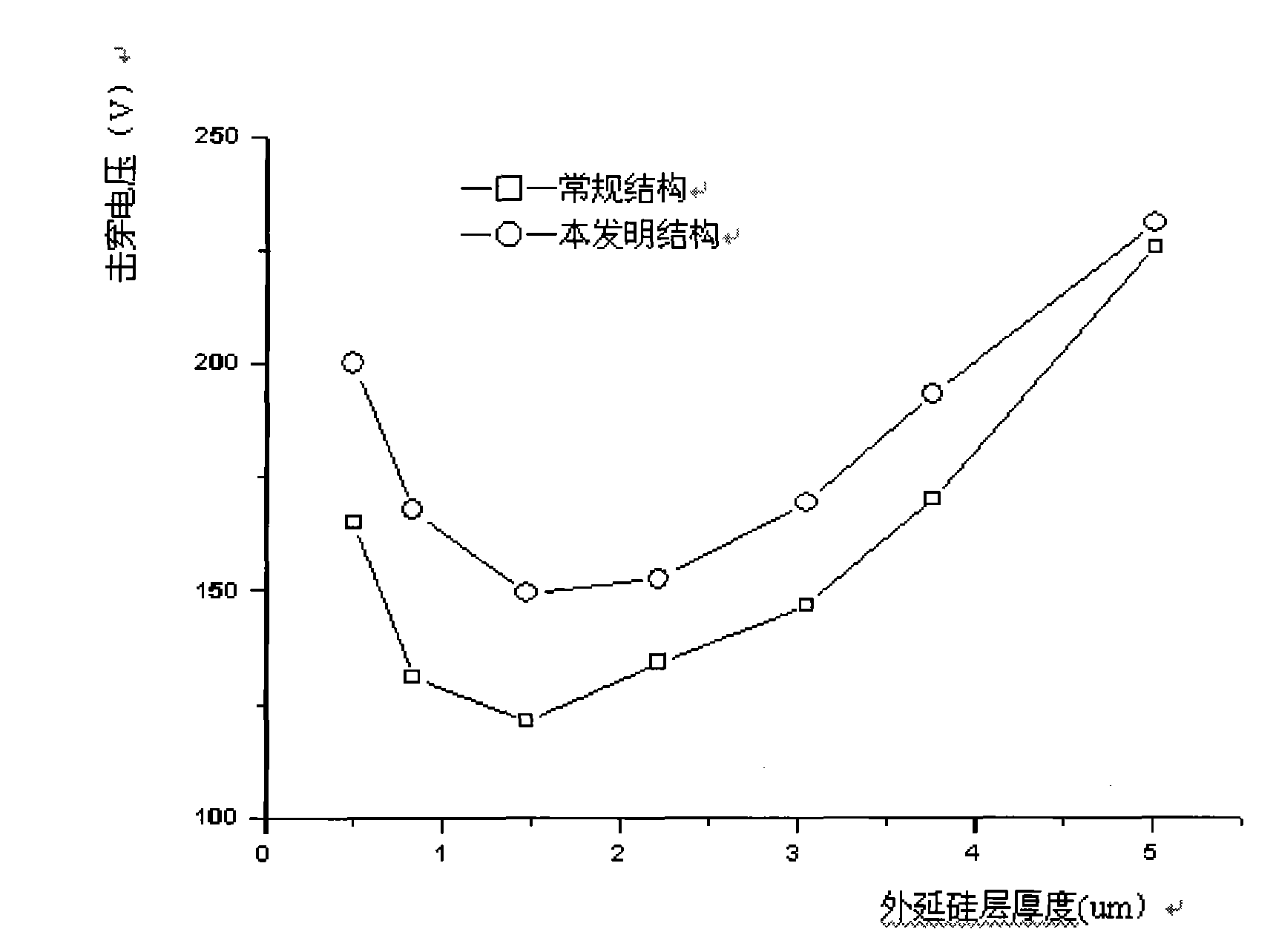
[0027] The lateral double-diffused metal-oxide-semiconductor transistor structure of a high-voltage N-type silicon-on-insulator with a conventional structure, such as figure 1 shown. However, the present invention provides an N-type silicon-on-insulator lateral double-diffused metal-oxide-semiconductor transistor that can effectively improve the withstand voltage of the device and reduce the on-resistance of the device.
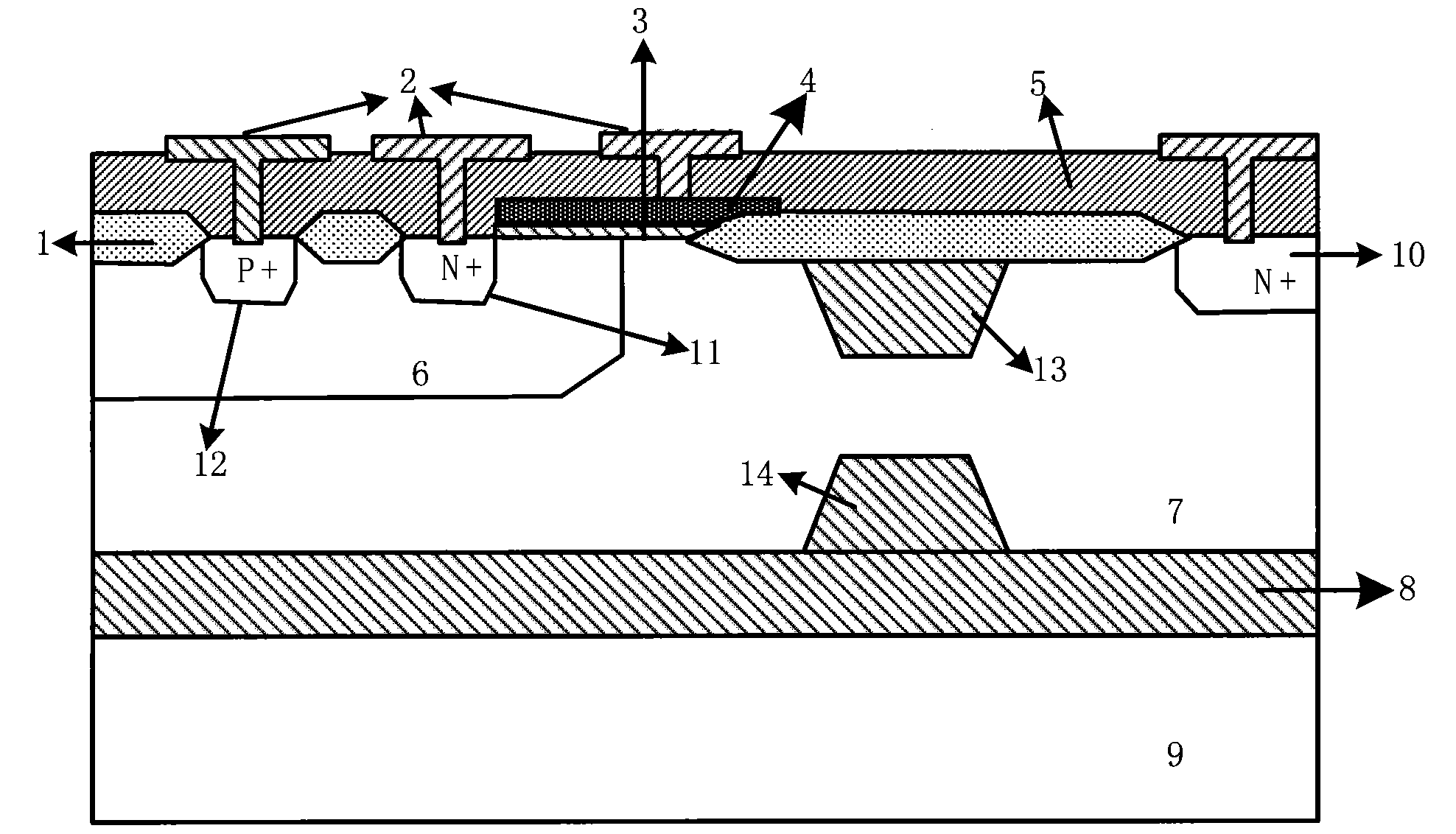
[0028] Such as figure 2 As shown, the N-type silicon-on-insulator lateral double-diffused metal oxide semiconductor transistor includes: a semiconductor substrate 9, a buried oxide layer 8 is arranged on the semiconductor substrate 9, and an N-type doped layer is arranged on the buried oxide layer 8. The semiconductor region 7 is provided with a P well 6 and an N type drain region 10 on the N type doped semiconductor region 7, and an N type source region 11 and a P type contact region 12 are arranged on the P well 6, and on the surface of the P well 6 A ga...
PUM
 Abstract
Description
Claims
Application Information