Si-Sb-Se phase changing thin-film material used for phase changing memory

A technology of phase change memory, si-sb-se, applied in the direction of static memory, digital memory information, information storage, etc., can solve the problem that the operation speed of phase change memory cannot be fast, the volume change of amorphous and polycrystalline transformation is large, and the unfavorable Long-term stable operation of the device and other issues, to achieve good data retention characteristics, fast crystallization speed, and good thermal stability

Active Publication Date: 2010-10-20
SHANGHAI INST OF MICROSYSTEM & INFORMATION TECH CHINESE ACAD OF SCI
View PDF0 Cites 0 Cited by
  • Summary
  • Abstract
  • Description
  • Claims
  • Application Information

AI Technical Summary

Problems solved by technology

But using Ge 2 Sb 2 Te 5 The phase change memory of the material has a large volume change between amorphous and polycrystalline transitions, and the set (SET) time is longer than 100ns, or even more than 300ns, which leads to Ge 2 Sb 2 Te 5 Phase-change memory of materials cannot operate very fast
Amorphous and polycrystalline transition volume changes greatly, which will affect the adhesion of the film and the electrode, which is not conducive to the long-term stable operation of the device
At the same time, Te element is superior to toxic elements, which is harmful to the environment, and is poorly compatible with CMOS technology

Method used


Image

  • Si-Sb-Se phase changing thin-film material used for phase changing memory
  • Si-Sb-Se phase changing thin-film material used for phase changing memory
  • Si-Sb-Se phase changing thin-film material used for phase changing memory

Examples


Embodiment 1

[0022] The Si-Sb-Se phase change film material provided by the present invention has a specific component of Si c Sb a Se b ,among them:

[0023] 48≤b≤60, 20≤a≤40, 8≤c≤40, a+b+c=100;

[0024] Preferably, the material composition of the Si-Sb-Se phase change film provided by the present invention is specifically Si 22 Sb 22 Se 56 , Si 14 Sb 29 Se 57 , Or Si 8 Sb 33 Se 59 .

[0025] Si c Sb a Se b Can also be expressed as Si y (Sb x Se 100-x ) 100-y form,

[0026] Among them, y=c, x(100-y)=a, and (100-x)(100-y)=b.

Embodiment 2

[0028] The Si-Sb-Se phase change film material provided by the present invention has a specific component of Si c Sb a Se b ,among them:

[0029] 60≤b≤80, 20≤a≤40, 3≤c≤20, a+b+c=100;

[0030] Preferably, when the expression form is (Sb x Se 1-x ) 1-y Si y When the material composition of the Si-Sb-Se phase change film provided by the present invention is specifically Si 10 (Sb 70 Se 30 ) 90 , Si 5 (Sb 70 Se 30 ) 95 .

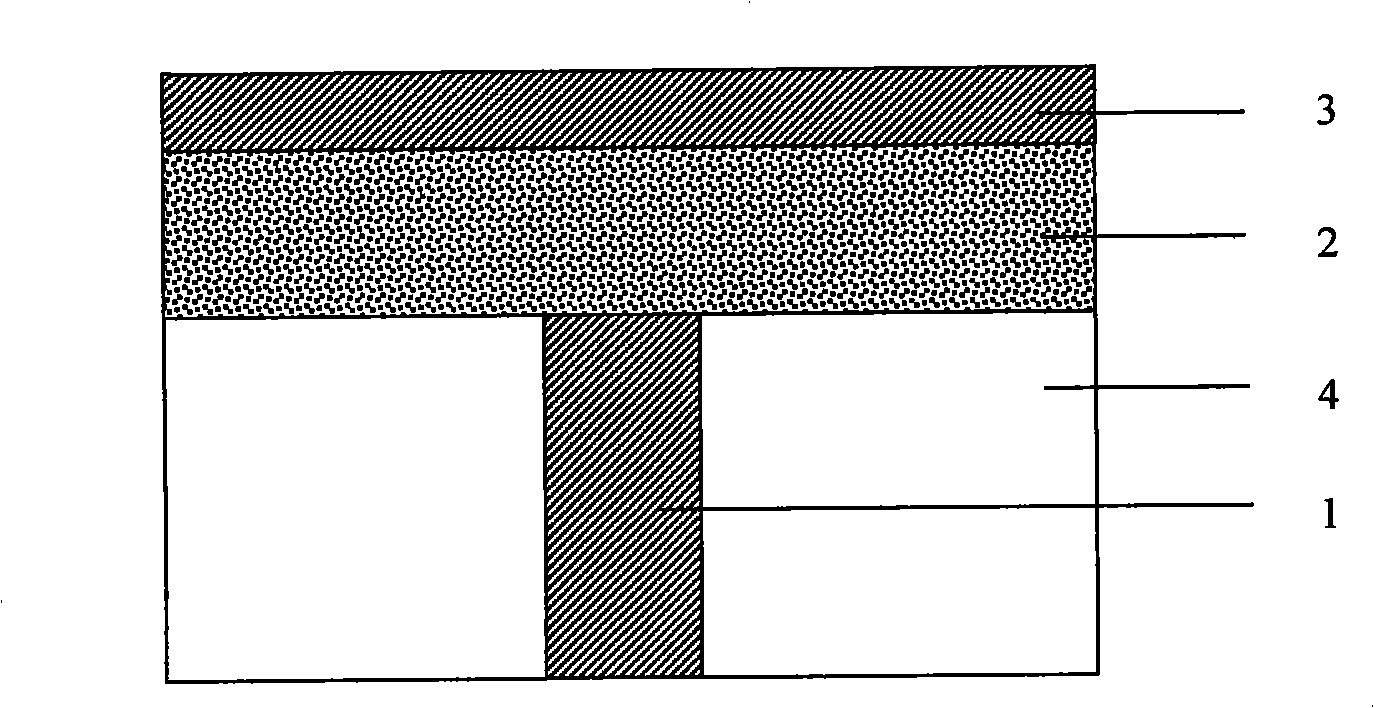
[0031] The Si-Sb-Se phase change film material of the present invention can be prepared by a multi-target co-sputtering method. The required component ratio can be obtained by adjusting the power corresponding to different targets. The Si-Sb-Se phase change film material can also be prepared by a single target sputtering method with an alloy target. The material can be prepared by chemical vapor deposition methods, including atomic layer deposition (ALD), or by electron beam evaporation, pulsed laser deposition, or by ion implantation of element Si in the Si-Sb-Se fi...


PUM


Abstract

The invention discloses a Si-Sb-Se phase transition film material used for a phase transition storage and the ingredient thereof is SicSbaSeb, wherein b is equal to or more than 48 and equal to or less than 60, a is equal to or more than 20 and equal to or less than 40, c is equal to or more than 8 and equal to or less than 40, and a plus b plus c is 100; or b is equal to or more than 60 and equal to or less than 80, a is equal to or more than 20 and equal to or less than 40, c is equal to or more than 3 and equal to or less than 20 and a plus b plus c is 100. Compared with the prior art, theSi-Sb-Se phase transition film material has faster crystallization rate, faster read-write rate and better data holding property than the commonly used Ge2Sb2Te5 material and better thermal stabilitythan SbSe binary material. Meanwhile, the material is free from element Te, thereby being environment friendly, and the material has good compatibility with the CMOS technique.

Description

technical field [0001] The invention relates to a phase-change thin film material in the field of microelectronics, in particular to a Si-Sb-Se phase-change thin film material used in a phase-change memory. Background technique [0002] Memory occupies an important position in the semiconductor market. Only DRAM (Dynamnic Random Access Memory) and FLASH occupy 15% of the entire market. With the gradual popularization of portable electronic devices, the market for non-volatile memory is also growing. At present FLASH occupies the mainstream of non-volatile memory, accounting for about 90%. However, with the advancement of semiconductor technology, FLASH has encountered more and more technical bottlenecks. First, the floating gate for storing charges cannot be thinned indefinitely with the development of integrated circuit technology. In addition, other shortcomings of FLASH technology also limit Its application, such as data writing is slow, high voltage is required when wri...

Claims


Application Information

Patent Timeline
Patent Type & Authority Patents(China)
IPC IPC(8): H01L45/00G11C11/56C22C12/00
Inventor 凌云龚岳峰宋志棠封松林
Owner SHANGHAI INST OF MICROSYSTEM & INFORMATION TECH CHINESE ACAD OF SCI
Why Eureka
Try Eureka