Photoelectric programmable multi-state memory based on thin film transistor structure and its preparation method

A thin-film transistor and memory technology, applied in the field of multi-state memory and its preparation, achieves the effects of low power consumption requirements, precise and controllable thickness, and low growth temperature

Active Publication Date: 2021-07-23
FUDAN UNIV
View PDF4 Cites 0 Cited by
  • Summary
  • Abstract
  • Description
  • Claims
  • Application Information

AI Technical Summary

Problems solved by technology

At present, there are few studies on the application of PQDs to memory devices

Method used


Image

  • Photoelectric programmable multi-state memory based on thin film transistor structure and its preparation method
  • Photoelectric programmable multi-state memory based on thin film transistor structure and its preparation method
  • Photoelectric programmable multi-state memory based on thin film transistor structure and its preparation method

Examples


Embodiment 1

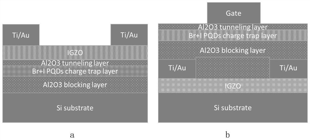
[0040] Embodiment 1 Bottom gate structure

[0041] Step 1, put the conductive substrate into the atomic layer deposition reaction chamber, the temperature range of the deposition chamber is 20°C-40°C, the temperature range of the TMA source bottle and each pipeline is 20°C-40°C, and vacuumize;

[0042] In step 2, an aluminum oxide barrier layer is prepared by atomic layer deposition. With trimethylaluminum and oxygen plasma as the reaction source, each cycle includes: 0.1s-2s trimethylaluminum pulse, 10s-30s nitrogen purge, 0.1s-10s oxygen plasma pulse, 10s-30s nitrogen purge sweep. Thickness range 30nm-50nm;

[0043] Step 3, with PbBr2, CsBr, PbI2, CsI, dimethylformamide, oleic acid, oleylamine, anhydrous toluene, methyl acetate, normal hexane etc., solution method prepares CsPbBr3, CsPbI3 perovskite quantum dot, and with Spin coating evenly on the barrier layer at a specific speed;

[0044] In step 4, an aluminum oxide tunneling layer is prepared by a low-temperature ato...

Embodiment 2

[0048] Example 2 Top Gate Structure

[0049] Step 1, put the substrate into the magnetron sputtering to grow the IGZO channel layer, define the channel pattern by ultraviolet lithography, and etch with dilute hydrochloric acid;

[0050] Step 2, define the pattern of the source and drain electrodes by photolithography again, remove the glue with acetone, and evaporate the Ti / Au source and drain electrodes by electron beam. Thickness range 70nm-130nm;

[0051] Step 3, put it into the atomic layer deposition reaction chamber, the temperature range of the deposition chamber is 20°C-40°C, the temperature range of the TMA source bottle and each pipeline is 20°C-40°C, and vacuumize;

[0052] In step 4, an aluminum oxide barrier layer is prepared by atomic layer deposition. With trimethylaluminum and oxygen plasma as the reaction source, each cycle includes: 0.1s-2s trimethylaluminum pulse, 10s-30s nitrogen purge, 0.1s-10s oxygen plasma pulse, 10s-30s nitrogen purge sweep. Thickne...


PUM

PropertyMeasurementUnit
thicknessaaaaaaaaaa
thicknessaaaaaaaaaa
thicknessaaaaaaaaaa

Abstract

The invention belongs to the technical field of semiconductor memory, in particular to a photoelectric programming multi-state memory based on a thin film transistor structure and a preparation method thereof. The invention realizes the multi-state memory under the photoelectric programming condition by introducing multiple perovskite quantum dots into the capture layer of the floating gate thin film transistor. The preparation method includes: placing a conductive substrate in an atomic layer deposition reaction chamber, and controlling the temperature of the deposition chamber; preparing an aluminum oxide barrier layer by low-temperature atomic layer deposition; preparing perovskite quantum dots by a solution method, and uniformly spin-coating them on the barrier layer; Aluminum oxide tunneling layer was prepared by low-temperature atomic layer deposition; IGZO channel layer was grown by magnetron sputtering, and the channel pattern was formed by photolithography; the second photolithography, Ti / Au source and drain electrodes were evaporated by electron beam, and the photoelectric programmable polymorphic memory. The invention can realize the multi-state storage behavior of the memory by changing the wavelength light during the voltage programming process. The invention provides a solution for research and development in the fields of multi-state storage, photoelectric detection, flexible electronics and the like.

Description

technical field [0001] The invention belongs to the technical field of semiconductor memory, and in particular relates to a multi-state memory and a preparation method thereof. Background technique [0002] With the continuous and rapid development of integrated circuit technology, people strongly hope to increase the data storage density of memory chips, and store a larger amount of data and information on smaller chips. In addition, artificial intelligence is gradually developing into a new generation of general-purpose technology, accelerating its penetration and integration with various economic and social fields. It has become the core frontier of new technological revolution and industrial transformation, and has become a new engine to promote economic and social development. In the field of artificial intelligence, the Internet of Things, social media, and security devices generate massive amounts of data, which require a large amount of memory to store, exchange, and...

Claims


Application Information

Patent Timeline
Patent Type & Authority Patents(China)
IPC IPC(8): H01L29/788H01L29/786H01L29/49H01L21/34G11C13/00
CPCG11C13/0007H01L29/4908H01L29/66969H01L29/7869H01L29/7887
Inventor 丁士进裴俊翔吴小晗张卫
Owner FUDAN UNIV
Why Eureka
Try Eureka