Structure of nanometer line cold-cathode electron source array with grid and method for producing the same as well as application of flat panel display
A manufacturing method and nanowire technology are applied in cold cathode manufacturing, electrode system manufacturing, discharge tube/lamp manufacturing, etc., to achieve the effects of high controllability and simple process
- Summary
- Abstract
- Description
- Claims
- Application Information
AI Technical Summary
Problems solved by technology
Method used
Image

Examples
Embodiment
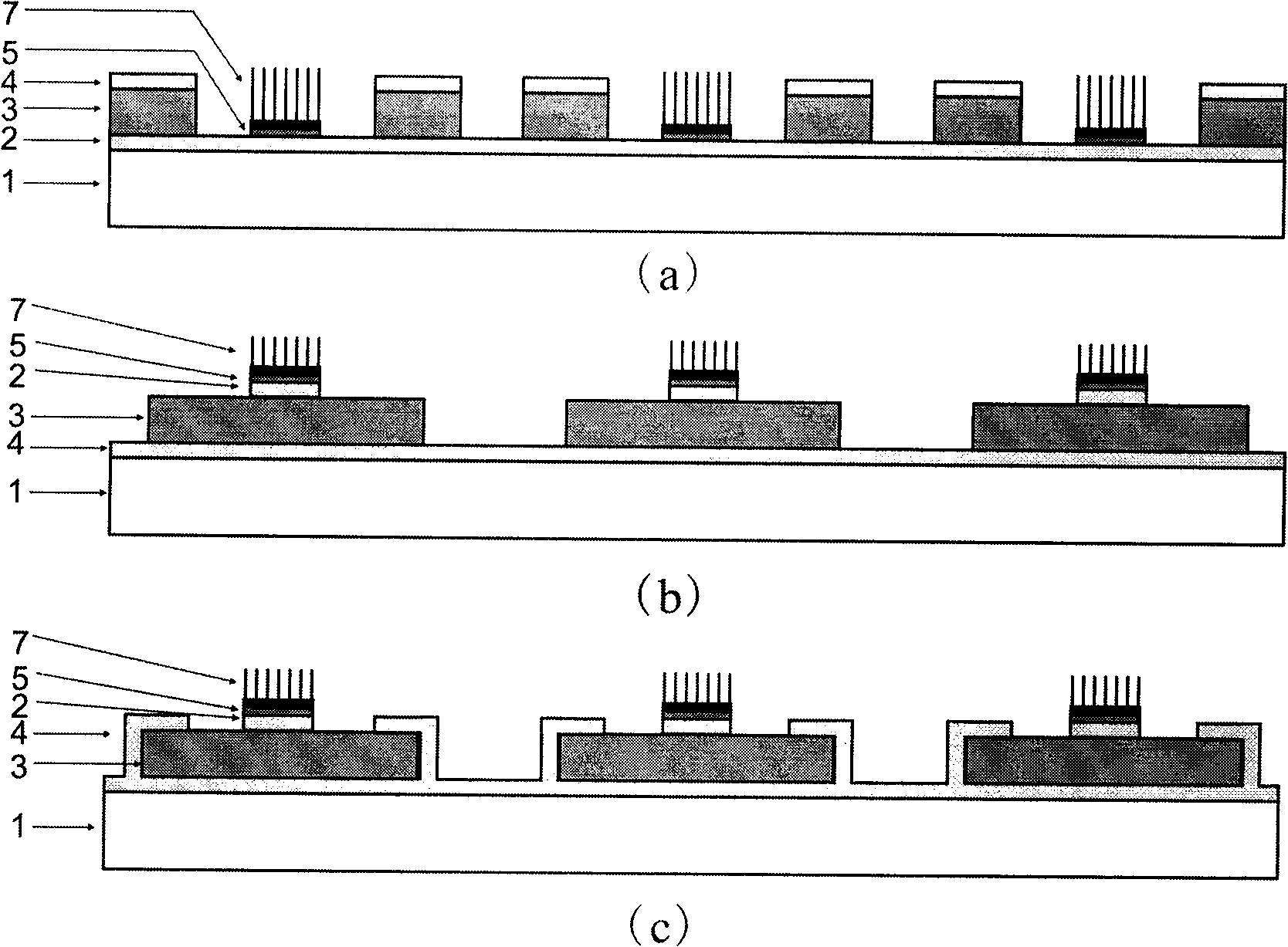
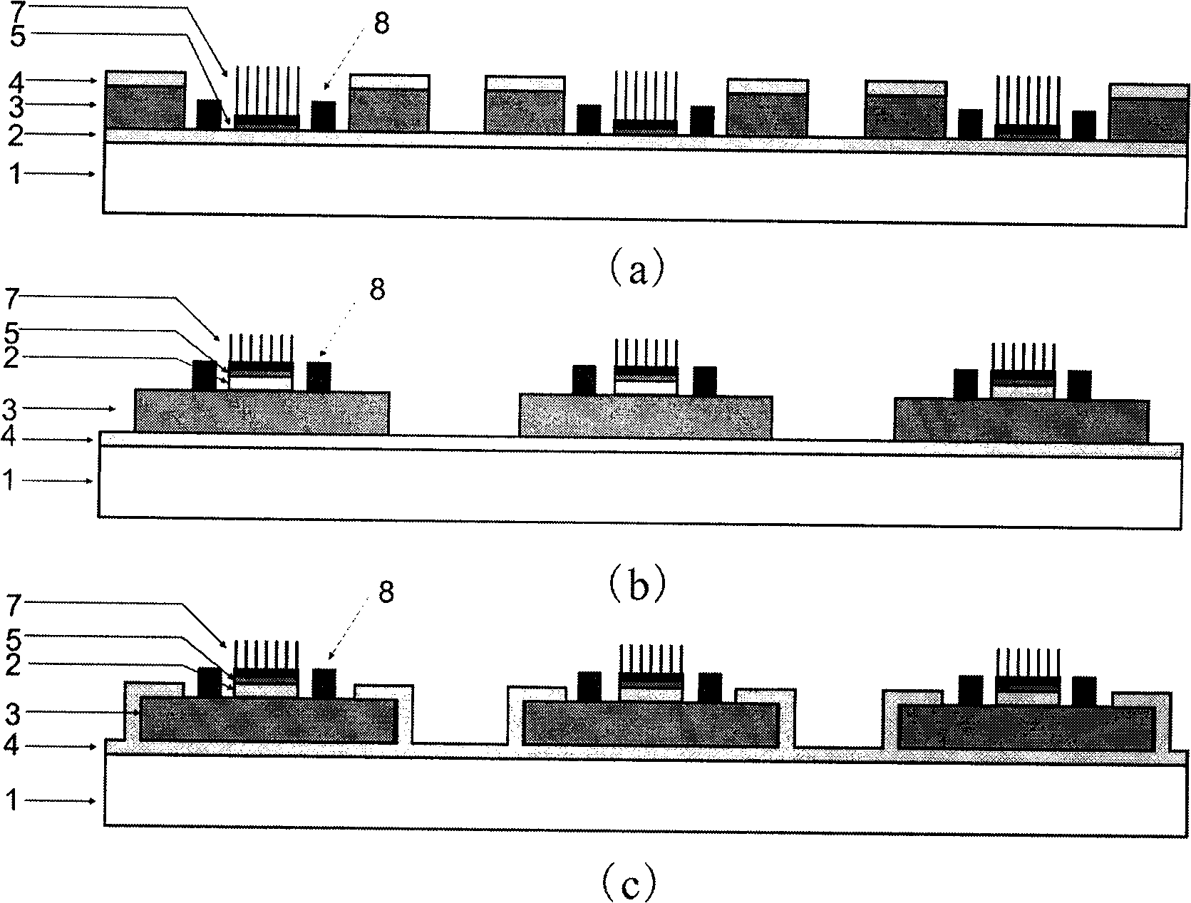
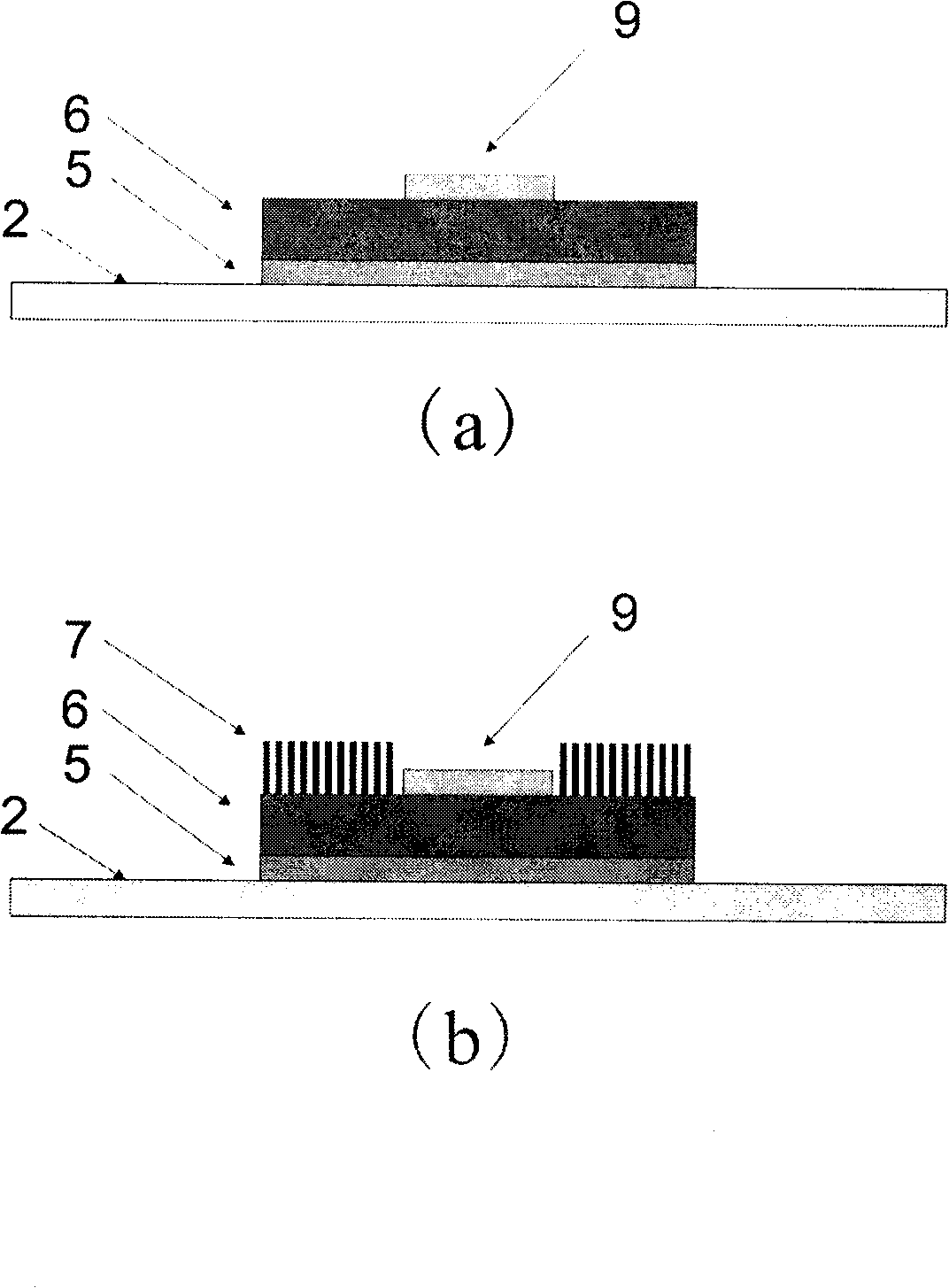
[0055] This example shows the fabrication process of an electron source array using copper oxide nanowires as the cold cathode material. For specific manufacturing process steps, please refer to the appendix Figure 7 . First, the glass substrate was ultrasonically cleaned with acetone, ethanol, and deionized water for 20 minutes, blown dry with nitrogen, and then dried. On the glass substrate, the cathode electrode strips were prepared by DC magnetron sputtering vacuum coating technology and stripping process. The cathode electrode strip is composed of chromium film and aluminum film, and its thickness is 120nm and 100nm, respectively. A composite insulating layer film of silicon nitride and silicon dioxide is prepared by plasma-enhanced vapor deposition, and its total thickness is 1.5 μm. The grid electrode strips were prepared by DC magnetron sputtering vacuum coating technology and stripping process. The gate electrode strips are composed of chromium film and aluminum ...
PUM
 Abstract
Description
Claims
Application Information