Electric bi-stable device based on composite film of semi-conductor nano crystalline and polymer

A technology of bistable devices and composite films, which is applied in semiconductor/solid-state device manufacturing, semiconductor devices, electric solid-state devices, etc., and can solve the problem of low current switching of electric bistable devices

Inactive Publication Date: 2009-08-12
BEIJING JIAOTONG UNIV
View PDF0 Cites 7 Cited by
  • Summary
  • Abstract
  • Description
  • Claims
  • Application Information

AI Technical Summary

Problems solved by technology

At present, reports on nanocrystalline and polymer electrical bistable devices mainly focus on the bistable devices of metal nanocrystals and polymer hybrid films, while there are fewer reports on bistable devices of semiconductor nanocrystals and polymer films, and Reported electrical bistable device with low current switching ratio

Method used


Image

  • Electric bi-stable device based on composite film of semi-conductor nano crystalline and polymer
  • Electric bi-stable device based on composite film of semi-conductor nano crystalline and polymer
  • Electric bi-stable device based on composite film of semi-conductor nano crystalline and polymer

Examples


Embodiment 1

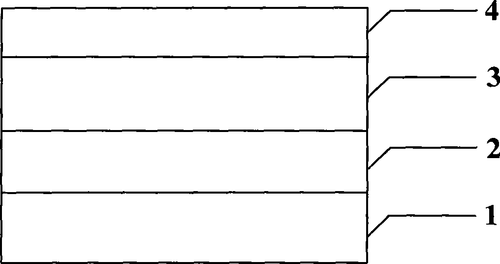
[0020] An electric bistable device based on a composite thin film of semiconductor nanocrystals and polymers. The device is made of indium tin oxide (ITO) conductive glass on a conductive substrate 1, and a buffer layer 2 is prepared by a spin-coating process. The spin-coated The speed is 5000 rpm. The functional active layer 3 above the buffer layer 2 is also prepared by a spin-coating process. This layer is made of cuprous sulfide nanocrystals and conjugated polymer poly(2-methoxy-5-(2) coated with dodecanethiol. -Ethylhexyloxy)-1,4-phenyleneethylene) mixed film, spin-coated at 1000 rpm. On top of the functional active layer 3 is a vacuum-evaporated aluminum electrode 4 .

[0021] Materials used in this example:

[0022] The material of the buffer layer 2 is sulfonated polystyrene-doped poly-3,4-ethylenedioxythiophene (PEDOT:PSS), and the thickness of the buffer layer 2 is 50 nm.

[0023] The material of the functional active layer 3 is cuprous sulfide nanocrystal coated ...

Embodiment 2

[0026] An electric bistable device based on a composite thin film of semiconductor nanocrystals and polymers. The device is made of indium tin oxide (ITO) conductive glass on a conductive substrate 1, and a buffer layer 2 is prepared by a spin-coating process. The spin-coated The speed is 5000 rpm. The functional active layer 3 above the buffer layer 2 is also prepared by a spin-coating process. This layer is made of cuprous sulfide nanocrystals and conjugated polymer poly(2-methoxy-5-(2) coated with dodecanethiol. -Ethylhexyloxy)-1,4-phenyleneethylene) mixed film, spin-coated at 1000 rpm. On top of the functional active layer 3 is a vacuum-evaporated aluminum electrode 4 .

[0027] Materials used in this example:

[0028] The material of the buffer layer 2 is poly-3,4-ethylenedioxythiophene doped with sulfonated polystyrene, and the thickness of the buffer layer 2 is 100 nm.

[0029] The material of the functional active layer 3 is cuprous sulfide nanocrystal coated with 7...


PUM

PropertyMeasurementUnit
thicknessaaaaaaaaaa
thicknessaaaaaaaaaa
thicknessaaaaaaaaaa

Abstract

The invention discloses an electric bistable device based on a composite film of a semiconductor nano-crystalline and a polymer, which relates to a photo-electronic device which has two different conduction states under the same voltage. The device comprises a conducting substrate (1) which is an ITO conducting glass and is sequentially manufactured with a buffer layer (2), a functional active layer (3) and an aluminum electrode (4). The material of the buffer layer (2) is sulfonated polystyrene doped poly-3,4-vinyl dioxy thiophene; and the material of the functional active layer (3) is the mixture of lauryl mercaptan coated cuprous sulfide nano-crystalline and conjugated polymer poly(2-methoxy-5-(2-ethylhexyloxy)-1,4-phenylene ethylene), and the ratio of the two components is between 1:1 and 3:1. The electric bistable device based on the composite film of the semiconductor nano-crystalline and the polymer has the characteristics of low cost, easy processing, thin film layer and high current switch ratio, thus the device has extensive application prospect in the field of information electronics industry in the future.

Description

technical field [0001] The invention belongs to the field of optoelectronic devices and relates to a bistable device using a composite material system of nano crystals and polymers. Background technique [0002] Electric bistability refers to the phenomenon of having two different conductive states at the same voltage. When an electric field is applied to both sides of the functional layer film, when the field strength reaches a certain value, the device can be transformed from a low-conductivity state to a high-conductivity state. By applying a reverse electric field, the device can be transformed from a high conduction state to a low conduction state. Devices based on electrical bistability are important electronic devices in the field of semiconductor electronics. In recent years, with the rapid development of optoelectronic devices such as organic electroluminescent devices, organic thin film transistors, and organic solar cells, organic bistable devices have also attra...

Claims


Application Information

Patent Timeline
Patent Type & Authority Applications(China)
IPC IPC(8): H01L51/00
Inventor 唐爱伟侯延冰钱磊滕枫
Owner BEIJING JIAOTONG UNIV
Why Eureka
Try Eureka