Method for manufacturing silica-based high-efficiency double-junction solar battery
A technology of solar cells and manufacturing methods, applied in the field of inorganic materials and solar cells, to achieve the effect of improving photoelectric conversion efficiency
- Summary
- Abstract
- Description
- Claims
- Application Information
AI Technical Summary
Problems solved by technology
Method used
Image
Examples
Embodiment Construction
[0027] Embodiment is described further in conjunction with accompanying drawing now:
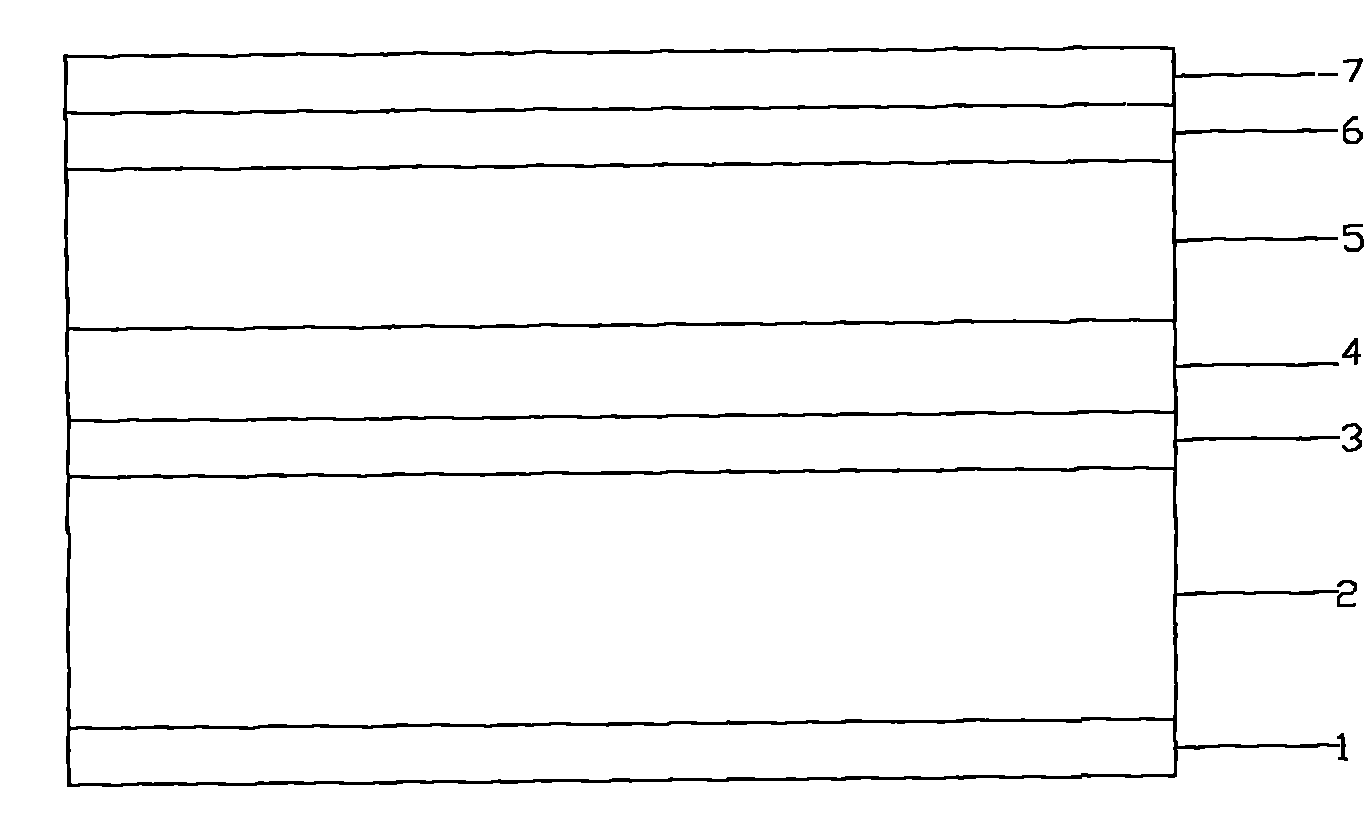
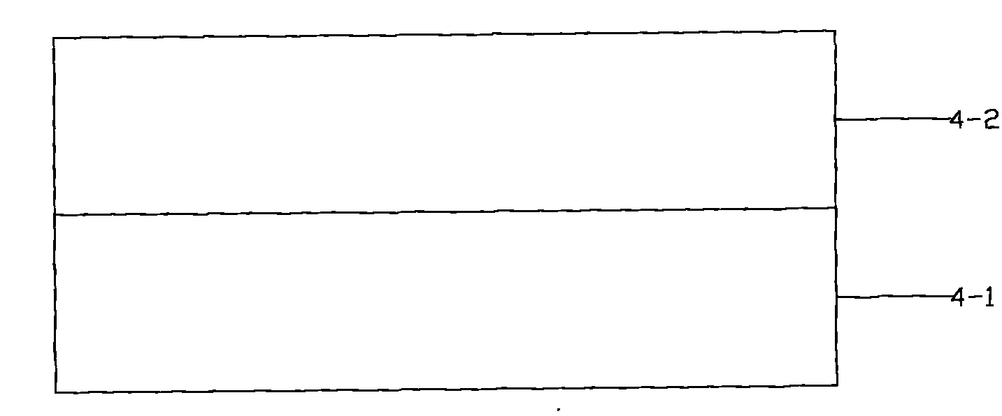
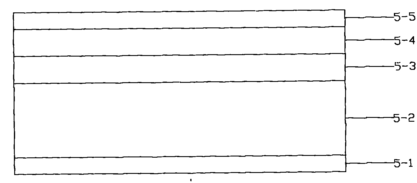
[0028] Such as figure 1 As shown, the structure of a double-junction solar cell is a Si / GaAs double-layer structure. The bottom cell 2 is a PN junction cell of Si, and the top cell 5 is a GaAs PN junction cell. The top cell 5 is directly epitaxially grown on the silicon cell substrate. superior.
[0029] Preparation method of silicon-based high-efficiency double-junction solar cells:
[0030] First, use 180μm-thick P-type monocrystalline silicon to make solar cells by chemical etching, and prepare high-efficiency textured surfaces in a magnetic field, that is, put monocrystalline silicon wafers into the textured surface preparation reactor prepared with a reaction solution for use For its reaction, the suede preparation reactor is placed in a magnetic field below 10T. The proportion of the reaction solution is: the mass percentage of sodium hydroxide or potassium hydroxide is 0.05% to 15%,...
PUM
 Abstract
Description
Claims
Application Information


