Aluminized BSF secondary sintering technology for crystal silicon solar cell

A solar cell and secondary sintering technology, which is applied to circuits, electrical components, semiconductor devices, etc., can solve the problems of surface silicon nitride film performance degradation, adverse effects on battery performance, and increased silicon body defects, etc., to achieve a simple and fast manufacturing process , good prospects for industrialization, and the effect of improving overall efficiency

Inactive Publication Date: 2009-09-23
SUN YAT SEN UNIV
View PDF0 Cites 11 Cited by
  • Summary
  • Abstract
  • Description
  • Claims
  • Application Information

AI Technical Summary

Problems solved by technology

However, in actual battery production, too high a sintering temperature will adversely affect the performance of other parts of the battery, such as increasing the propagation and diffusion of silicon defects and impuri...

Method used


Image

  • Aluminized BSF secondary sintering technology for crystal silicon solar cell
  • Aluminized BSF secondary sintering technology for crystal silicon solar cell
  • Aluminized BSF secondary sintering technology for crystal silicon solar cell

Examples


Embodiment 1

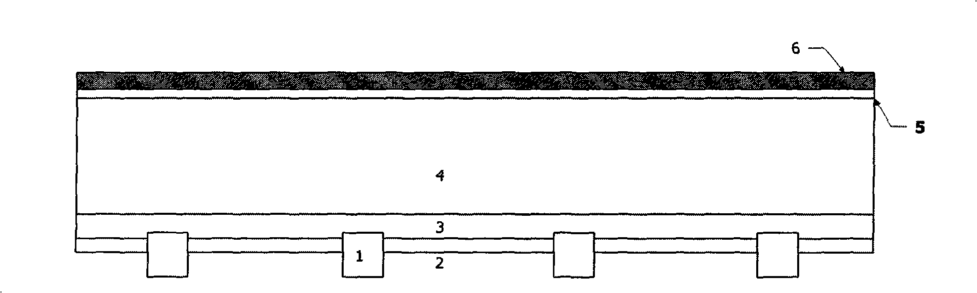
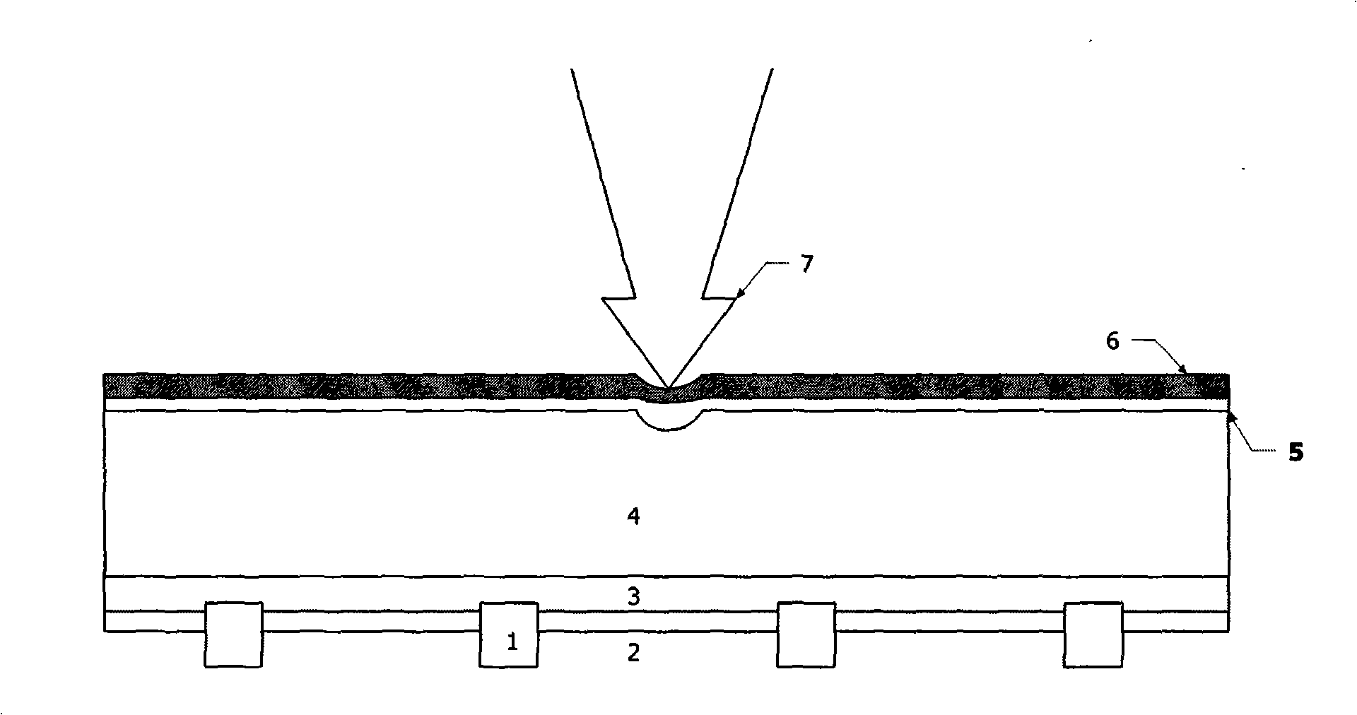
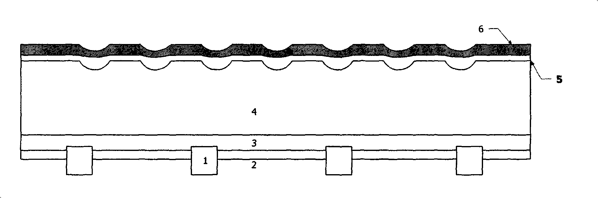
[0025] A Nd:YAG laser with a wavelength of 1064nm is used: the laser pulse frequency is 1K-30KHz, the galvanometer scans, and the transverse mode of the beam is a low-order mode. Set the laser pulse frequency to 1-10KHz, the scanning speed to 100mm / s, and the excitation current to 16-21A. The sample is a finished conventional p-type crystalline silicon cell using a screen printing process. The sintering scanning pattern is a dense lattice, local sintering, the spot diameter is about 80 microns, and the spacing is about 0.5mm. The laser beam is sintered by repeating multiple pulses at one point.

Embodiment 2

[0027] A Nd:YAG laser with a wavelength of 1064nm is used: the laser pulse frequency is 1K-30KHz, the galvanometer scans, and the transverse mode of the beam is a low-order mode. Set the laser pulse frequency to 1-15KHz, the scanning speed to 100mm / s, and the excitation current to 16-25A. The sample is a finished conventional p-type crystalline silicon cell using a screen printing process. The sintering scanning pattern is a dense circle array, partially sintered, the diameter of the circle is 100-200 microns, and the spacing is about 0.5-1mm. The laser beam scans along the circle, which can be repeated many times according to the actual performance.

Embodiment 3

[0029] A Nd:YAG laser with a wavelength of 1064nm is used: the laser pulse frequency is 1K-30KHz, the galvanometer scans, and the light-speed transverse mode is a low-order mode. Set the laser pulse frequency to 1-10KHz, the scanning speed to 20-200mm / s, and the excitation current to 18-25A. The sample is a finished conventional p-type crystalline silicon cell using a screen printing process. The sintering scanning pattern is an array of parallel lines with a line spacing of about 50-200 microns, and the laser sintering covers the entire aluminum layer on the back of the battery.


PUM


Abstract

The invention discloses an aluminized BSF secondary sintering technology for a crystal silicon solar cell. The technology utilizes a laser beam or a microwave beam in a pulse mode to scan or integrally scan an aluminized BSF region at the back of the cell so that aluminum in a scanning region is instantaneously heated and melted and diffuses to a silica body; and a whole or partial aluminum heavily-doped region is formed at the back of the solar cell so as to form a BSF with excellent performance, thereby accelerating the diffusion of minority carriers, improving the collection ratio of the minority carriers, improving the long-wave response of the cell and further improving the whole efficiency of the cell. The technology can control the thermal influence of secondary sintering on the periphery of an aluminum layer so as not to generate obvious adverse influence on other parts of the cell, has various flexible laser sintering design modes, is simple, convenient and rapid to manufacture and can be rapidly combined with the prior industrial production.

Description

technical field [0001] The invention relates to a method for secondary sintering of an aluminum back field of a crystalline silicon solar cell, in particular to a method for secondary sintering of an aluminum layer on the back of a polycrystalline silicon solar cell by using a pulse heat source such as laser or microwave to form a high-performance aluminum back field method. Background technique [0002] Silicon solar cells use p-n junction photovoltaic effect to realize photoelectric conversion, which has become one of the mainstreams of new energy development. In 2008, crystalline silicon solar cells accounted for about 90% of the world's total output of solar cells, and will continue to occupy the mainstream position in the market for a period of time in the future. Most of the crystalline silicon solar cells are made of p-type silicon wafers, and the back is screen-printed. The aluminum layer diffuses aluminum into the silicon matrix through a rapid sintering furnace to...

Claims


Application Information

Patent Timeline
IPC IPC(8): H01L31/18
CPCY02P70/50
Inventor 沈辉王学孟张陆成
Owner SUN YAT SEN UNIV
Why Eureka
Try Eureka