Silicon base grown AlGaInP LED epitaxial wafer and preparation method thereof
A technology of LED epitaxial wafers and aluminum gallium indium phosphide, which is applied in the field of optoelectronics, can solve the problems of low luminous efficiency of light-emitting diodes, and achieve the effects of improving high-current working ability, large size, and mature preparation technology
- Summary
- Abstract
- Description
- Claims
- Application Information
AI Technical Summary
Problems solved by technology
Method used
Image

Examples
Embodiment 1
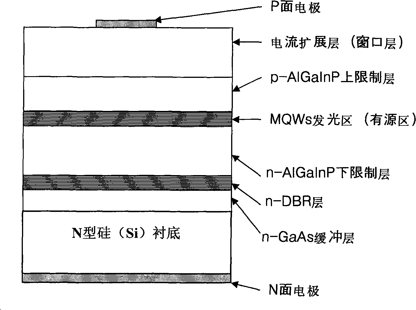
[0029] Such as figure 1As shown, the silicon substrate in the AlGaInP LED epitaxial wafer grown on the silicon substrate of this embodiment adopts N-type silicon material, and the n-type GaAs buffer layer (arsenic) is sequentially included on the silicon substrate from bottom to top. GaN low-temperature buffer layer and GaAs high-temperature buffer layer), n-type DBR reflective layer, n-type AlGaInP lower confinement layer, multiple quantum wells (MQWs) light-emitting region (active region), p-type aluminum Gallium indium phosphide upper confinement layer, p-type current expansion layer (window layer), and then use the die preparation technology to produce an LED chip with the P-side electrode (positive electrode) on the top and the N-side electrode (negative electrode) on the bottom.
[0030] The preparation method of the AlGaInP LED epitaxial wafer grown on the above silicon substrate comprises the following steps:
[0031] (1) Silicon substrate preparation: first place the...
Embodiment 2
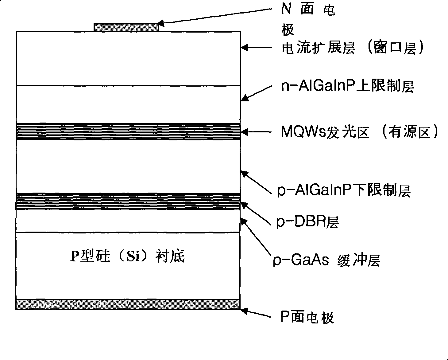
[0042] Such as figure 2 As shown, the silicon substrate in the AlGaInP LED epitaxial wafer grown on the silicon substrate of this embodiment adopts a p-type silicon material, and a p-type gallium arsenide buffer layer (arsenic GaN low-temperature buffer layer and GaAs high-temperature buffer layer), p-type DBR reflective layer, p-type AlGaInP lower confinement layer, multiple quantum wells (MQWs) light-emitting region (active region), n-type aluminum Gallium indium phosphide upper confinement layer, n-type current expansion layer (window layer), and then use the die preparation technology to manufacture LED chips with the N-side electrode (negative electrode) on the top and the P-side electrode (positive electrode) on the bottom.
[0043] The preparation method of the AlGaInP LED epitaxial wafer grown on the above silicon substrate comprises the following steps:
[0044] (1) Carry out silicon substrate preparation and heat treatment by the process described in embodiment 1; ...
Embodiment 3
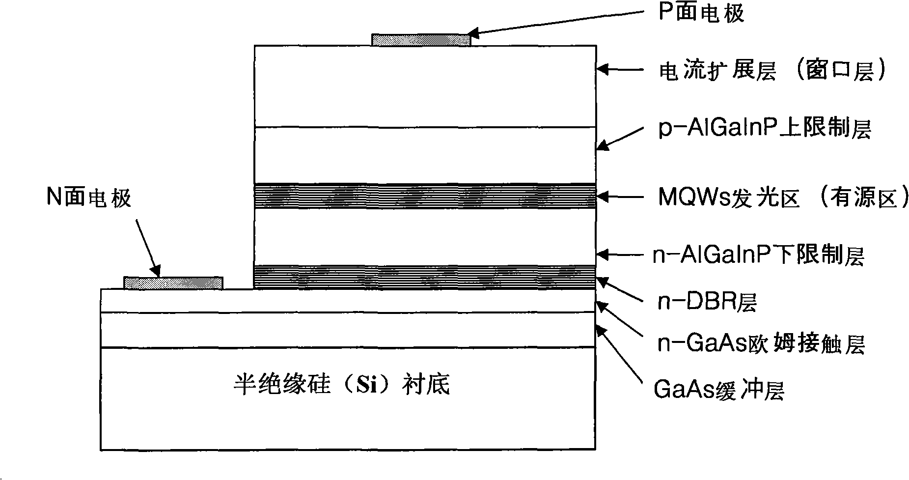
[0054] Such as image 3As shown, the silicon substrate in the AlGaInP LED epitaxial wafer grown on the silicon substrate of this embodiment adopts semi-insulating silicon material, and the silicon substrate 1 includes a gallium arsenide buffer layer (arsenide Gallium low-temperature buffer layer and gallium arsenide high-temperature buffer layer), n-type gallium arsenide ohmic contact layer, n-type DBR reflective layer, n-type aluminum gallium indium phosphorus lower confinement layer, multiple quantum wells (MQWs) light emitting region ( Active region), p-type aluminum gallium indium phosphorus upper confinement layer, p-type current spreading layer (window layer), and then use the die preparation technology to make the P-side electrode (positive electrode) and N-side electrode (negative electrode) on the same top LED chips.
[0055] The preparation method of the AlGaInP LED epitaxial wafer grown on the above silicon substrate comprises the following steps:
[0056] (1) Car...
PUM
 Abstract
Description
Claims
Application Information
 - R&D
- Intellectual Property
- Life Sciences
- Materials
- Tech Scout
- Unparalleled Data Quality
- Higher Quality Content
- 60% Fewer Hallucinations
Browse by: Latest US Patents, China's latest patents, Technical Efficacy Thesaurus, Application Domain, Technology Topic, Popular Technical Reports.
© 2025 PatSnap. All rights reserved.Legal|Privacy policy|Modern Slavery Act Transparency Statement|Sitemap|About US| Contact US: help@patsnap.com