Method for implementing gallium nitride thin film low temperature deposition on silicon substrate

A technology of silicon substrate and gallium nitride, which is applied in the direction of electrical components, circuits, semiconductor devices, etc., can solve the problems of limiting the application and promotion of gallium nitride materials, lattice mismatch, poor heat dissipation performance, etc., and achieve the problem of thermal expansion coefficient mismatch Matching problems, improving application level, and good practical effects

Pending Publication Date: 2009-02-18
SOUTH CHINA NORMAL UNIVERSITY
View PDF0 Cites 9 Cited by
  • Summary
  • Abstract
  • Description
  • Claims
  • Application Information

AI Technical Summary

Problems solved by technology

Sapphire is currently the most commonly used substrate material, and the preparation process is relatively mature, but sapphire itself is not conductive, has poor heat dissipation performance, and has a large difference in lattice constant and thermal expansion coefficient compared with gallium nitride materials. The application of gallium nitride materials has been promoted; the limitation of silicon carbide substrates is that it is expensive; the lattice constant and thermal expansion coefficient of aluminum nitride are close to those of gallium nitride, but the single crystal size obtained now is too small, which limits The application of gallium nitride materials; silicon has the advantages of high quality, large size, high thermal conductivity, and low cost. If silicon is used as a substrate, it is very possible to integrate gallium nitride-based devices into silicon-based large-scale integrated circuits , so silicon is considered to be the most promising ideal substrate material for preparing gallium nitride thin films. However, due to the problems of lattice mismatch and thermal expansion mismatch in silicon substrates, the application research on it is still in the international arena. In the immature research stage, there is no mature and feasible method for preparing gallium nitride thin films

Method used


Image

  • Method for implementing gallium nitride thin film low temperature deposition on silicon substrate

Examples


Embodiment Construction

[0027] In the preparation of blue light-emitting materials such as gallium nitride, metal-organic chemical vapor deposition (MOCVD) and molecular beam epitaxy (MBE) are widely used at home and abroad to deposit on sapphire and silicon carbide substrates. The purpose of the present invention is to improve this and promote the industrialization of gallium nitride thin film materials. The specific method is as follows:

[0028] 1) Using the Langmuir probe to diagnose the spatial distribution of the ECR plasma

[0029] 2) Use a grating monochromator to analyze the emission spectrum of the groups in the ECR plasma

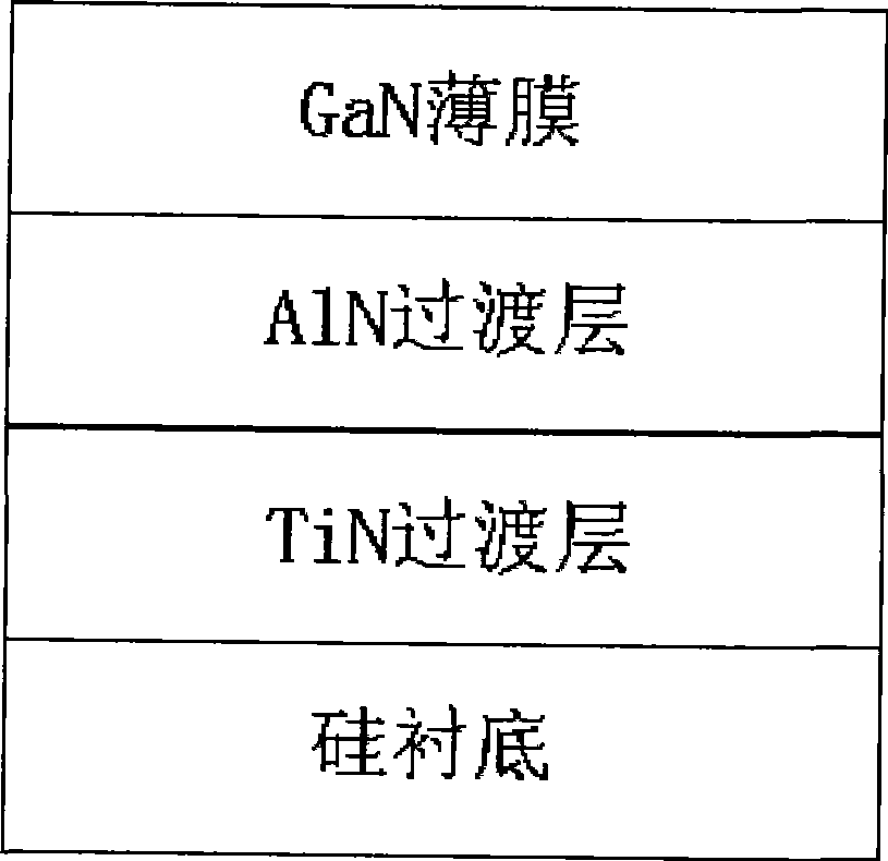
[0030] 3) As shown in FIG. 1, a TiN transition layer is first grown on the silicon substrate by plasma-assisted electron beam evaporation reaction deposition or other methods, and the thickness of the transition layer is about 30-50 nm. In this embodiment, the thickness of the transition layer is about 50 nm.

[0031] 4) Using ethyl aluminum (TEAl), dimethyl zinc (DM...


PUM

PropertyMeasurementUnit
thicknessaaaaaaaaaa
thicknessaaaaaaaaaa

Abstract

This invention is a method for realizing low temperature deposition of gallium nitride film on a silicon substrate, including following steps: 1) diagnosing the space distribution of an ECR plasma; 2) processing emission spectrum analysis to the group of the ECR plasma; 3) firstly depositing a layer of TiN transition layer on the silicon substrate; 4) preparing an A1N transition layer doped with gradually changed structure on the silicon substrate; 5) preparing a GaN cushion layer doped with gradually changed structure on the TiN transition layer, and externally extending to grow a crystal GaN film under low temperature on the GaN cushion layer doped with the gradually changed structure; depositing a GaN film under lower temperature on the A1N transition layer. This invention has excellent practicability and better guarantees the high quality of the GaN film through depositing the GaN film under low temperature.

Description

technical field [0001] The invention relates to a method for realizing low-temperature deposition of gallium nitride thin film on a silicon substrate, which belongs to the transformation technology of the method for realizing low-temperature deposition of gallium nitride thin film on a silicon substrate. Background technique [0002] Wide bandgap direct semiconductor materials represented by gallium nitride thin films have attracted international attention in recent years. Small size, stable chemical properties, radiation resistance, high temperature resistance, etc., make it widely used in optoelectronic devices such as high-brightness blue light-emitting diodes (LEDs), blue lasers, and ultraviolet detectors, as well as electronic devices such as radiation resistance, high frequency, high temperature, and high voltage. Huge application market prospects. [0003] In the preparation of blue light-emitting materials such as gallium nitride, metal-organic chemical vapor deposi...

Claims


Application Information

Patent Timeline
Patent Type & Authority Applications(China)
IPC IPC(8): H01L33/00H01L21/20H01L21/205
Inventor 陈俊芳李炜孟然薛永奇王燕
Owner SOUTH CHINA NORMAL UNIVERSITY
Why Eureka
Try Eureka