Method for preparing neuro chip by taking polylactic acid as substrate

A neural chip and polylactic acid technology, which is applied in photoplate-making process coating equipment, micro-lithography exposure equipment, photoplate-making process exposure devices, etc., can solve the problem that single-crystal silicon wafers do not have biocompatibility and affect the working life of chips, etc. problem, to achieve the effect of stable working life, prolonging life, and strong biocompatibility

Inactive Publication Date: 2009-09-30
SHANGHAI JIAO TONG UNIV
View PDF0 Cites 4 Cited by
  • Summary
  • Abstract
  • Description
  • Claims
  • Application Information

AI Technical Summary

Problems solved by technology

But the disadvantage is that the monocrystalline silicon wafer does not have good biocompatibility, which will affect

Method used


Image

  • Method for preparing neuro chip by taking polylactic acid as substrate

Examples


Embodiment Construction

[0024] Embodiments of the present invention are described in detail below in conjunction with the accompanying drawings: this implementation is carried out under the premise of the technical solution of the present invention, and detailed implementation methods and specific operating procedures have been provided, but the protection scope of the present invention is not limited to the following the described embodiment.

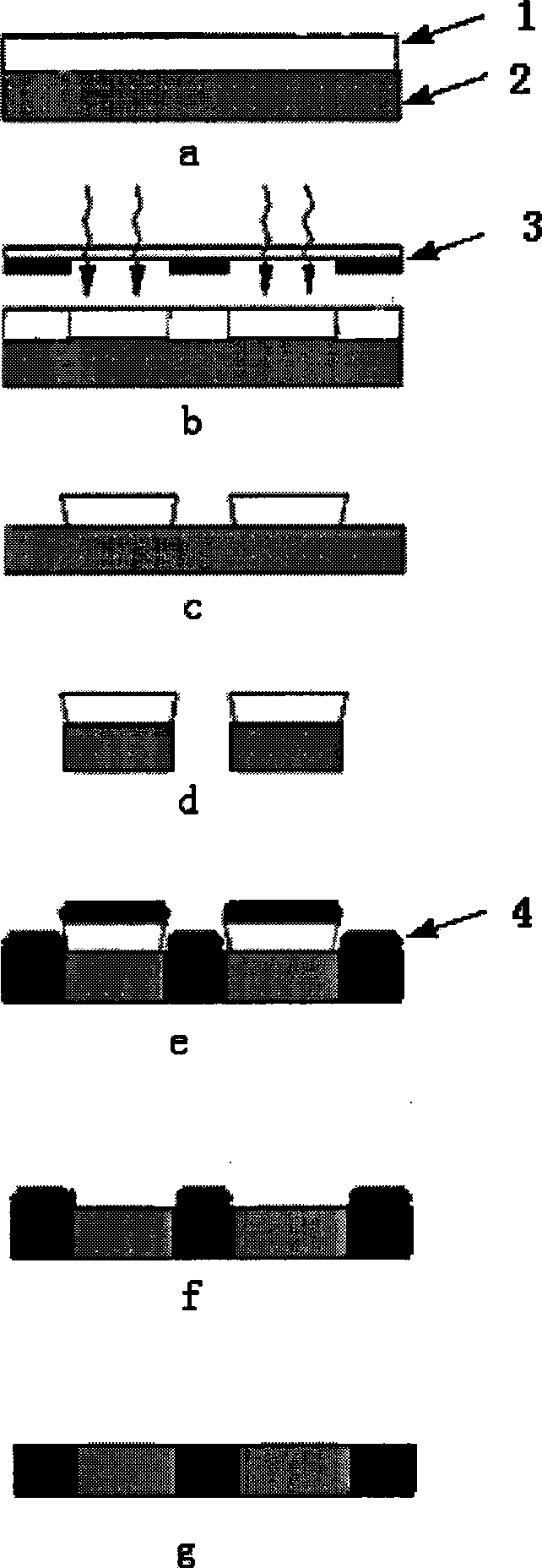
[0025] Such as figure 1 As shown, it is a process flow diagram of the present invention, wherein: a is to spin coat a layer of photoresist on the polylactic acid substrate; b is to carry out UV exposure to the photoresist after spin coating; after c exposure, the device is put into developing solution, remove the unexposed photoresist part; d is to etch a circular hole on the polylactic acid substrate with NaOH etchant; e is sputtering gold; f is removing the exposed photoresist from the sputtered gold device At the same time, the sputtered gold on the photo...


PUM


Abstract

The invention relates to a method for preparing a neuro chip by taking polylactic acid as a substrate in the technical field of biological engineering. The method comprises the following steps: firstly, spin coating of a layer of photoresist on the polylactic acid substrate; secondly, carrying out UV exposure on the photoresist subjected to spin coating; thirdly, placing the exposed device in a developing solution to remove the part of unexposed photoresist; fourthly, etching a round hole on the polylactic acid substrate by a NaOH etching agent; fifthly, sputtering gold in the round hole of the polylactic acid substrate; sixthly, removing the exposed photoresist from the device which is sputtered by the gold, and peeling off the sputtered gold on the photoresist; and seventhly, carrying out chemical mechanical planarization to ensure that the gold and an integrated circuit are well connected with each other. The method adopts the polylactic acid substrate instead of a monocrystalline silicon substrate, not only can realize functions of the prior neuro chip, but also can realize excellent biological compatibility and stable working life, compared with the prior neuro chip.

Description

technical field [0001] The invention relates to a method for preparing a chip in the technical field of bioengineering, in particular to a method for preparing a neurochip based on polylactic acid. Background technique [0002] The neural chip technology was proposed by scientists from the University of Padua in Italy on March 27, 2006. This research will help to develop advanced nerve repair technology for the treatment of nerve disorders or develop living nerve cells Organic computers that process data. The specific principle is as follows: 16,000 electronic transistors and hundreds of capacitors are installed on a silicon chip with a size of 1 square millimeter, and then brain cells are glued to the chip with a special protein found in the brain. The ion channels of the nerve cells are connected to the semiconductor material so that the nerve cell's electrical signals can be transmitted to the silicon chip. Through this protein, the electronic components on the neurochi...

Claims


Application Information

Patent Timeline
IPC IPC(8): A61N1/36A61F2/00G03F7/16G03F7/20G03F7/26C23C14/34C23C14/20
Inventor 李以贵陈少军张冠孙健高阳
Owner SHANGHAI JIAO TONG UNIV
Why Eureka
Try Eureka