Alignment system for lithography equipment, lithography equipment and aligning method thereof

An alignment system and alignment light technology, applied in the field of alignment systems, can solve problems such as the decrease of the signal-to-noise ratio of the alignment signal, the asymmetric deformation of the alignment signal, and the surface of the wafer is not too rough, so as to improve the strength of the alignment signal , Reduce the alignment position deviation, suppress the effect of destructive interference effect

Inactive Publication Date: 2009-10-07
SHANGHAI MICRO ELECTRONICS EQUIP (GRP) CO LTD
View PDF2 Cites 30 Cited by
  • Summary
  • Abstract
  • Description
  • Claims
  • Application Information

AI Technical Summary

Problems solved by technology

[0009] However, the LSA alignment system is only suitable for processes where the wafer surface is not too rough and there is no asymmetric deformation of the alignment marks
LSA can achieve high-precision and high-yield alignment performance before the metal layer. For the metal layer, because the surface is very rough, there are many metal particles (about 1 μm), and the resulting stray light enters the LSA alignment system. of the photodetector, resulting in a decrease in the signal-to-noise ratio of the alignment signal
At the same time, the asymmetric deformation of the LSA mark caused by metal sputtering makes the alignment signal also asymmetrically deformed, resulting in alignment position deviation
In addition, the LSA alignment system judges the alignment position based on the amplitude signal of the diffraction light intensity. For shallow groove marks, due to the decrease in the diffraction efficiency of the grating mark, the alignment signal intensity will decrease, resulting in a decrease in the signal-to-noise ratio of the alignment signal.

Method used


Image

  • Alignment system for lithography equipment, lithography equipment and aligning method thereof
  • Alignment system for lithography equipment, lithography equipment and aligning method thereof
  • Alignment system for lithography equipment, lithography equipment and aligning method thereof

Examples


Embodiment Construction

[0037] In order to better understand the technical content of the present invention, specific embodiments are given together with the attached drawings for description as follows.

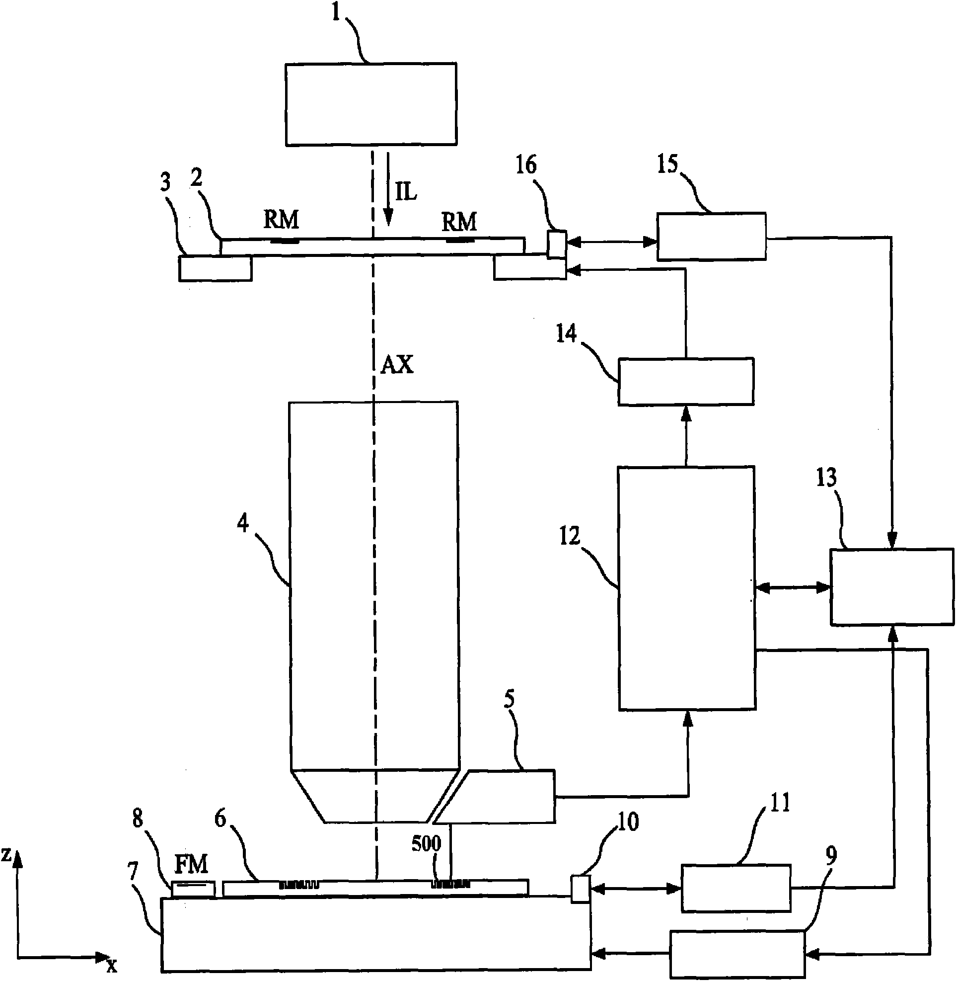
[0038] figure 1 It is a schematic diagram of the overall layout and working principle structure between the alignment system of the lithography apparatus of the present invention and the lithography apparatus.

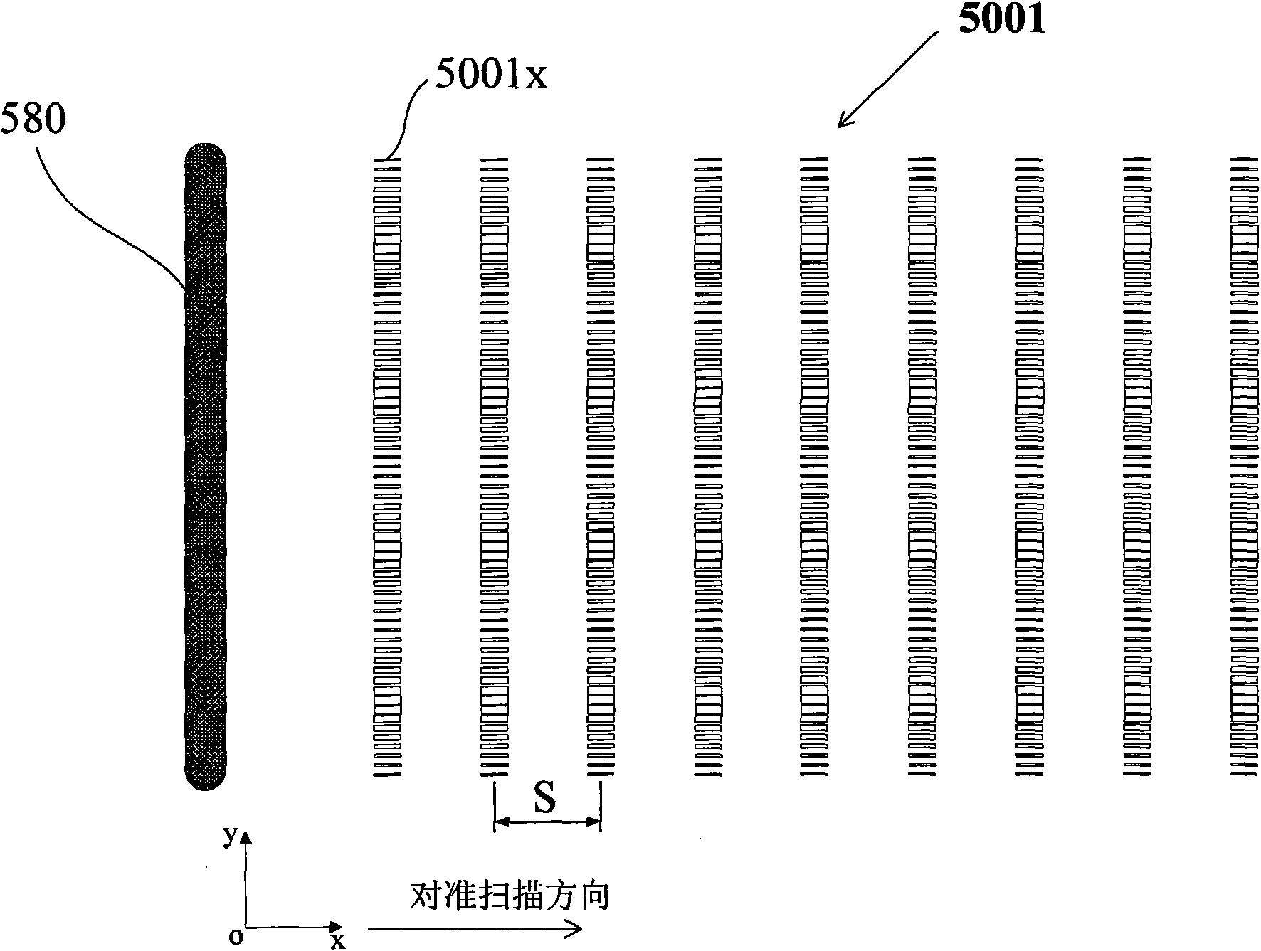
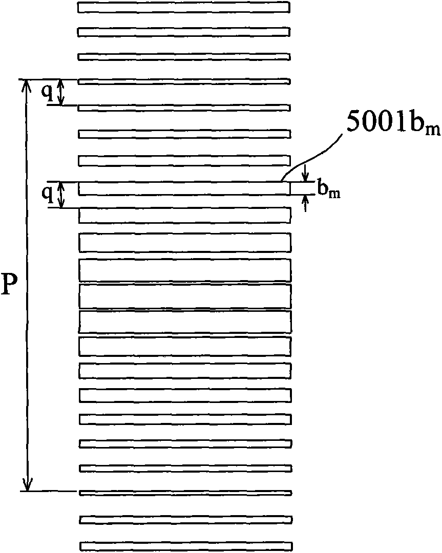
[0039] The composition of the lithography apparatus in this embodiment includes: an illumination system 1 for providing an exposure light beam; a mask holder and a mask table 3 for supporting a reticle 2, and the reticle 2 has a mask pattern and a periodic structure The mask alignment mark RM of the mask; the projection optical system 4 for projecting the mask pattern on the reticle 2 onto the wafer 6; the wafer holder and the wafer stage 7 for supporting the wafer 6, and the wafer stage 7 is engraved with fiducials Reference plate 8 labeled FM, alignment marks 500 with periodic optical st...


PUM


Abstract

The invention provides an alignment system for lithography equipment used for aligning a wafer according to alignment mark of the wafer, comprising a light source module, a lightening module, an imaging module, a detection module, and a single processing and positioning module. The alignment mark is an array structure comprising a plurality of column raster and line raster, wherein line width or duty ratio of the column rasters or linear rasters is changed in sine manner is raster period, and illuminating beams illuminate N column rasters or linear rasters of the alignment mark in turn. The alignment system in the invention can eliminate aligned position deviation, thereby improving the alignment precision.

Description

technical field [0001] The present invention relates to an alignment system, and in particular to an alignment system for a photolithography device, and also to a photolithography device using the alignment system and an alignment method thereof. Background technique [0002] The photolithography apparatus in the prior art is mainly used in the manufacture of integrated circuits (ICs) or other micro devices. Through photolithography equipment, multi-layer masks with different mask patterns are sequentially imaged under precise alignment on a wafer coated with photoresist, such as a semiconductor wafer or an LCD liquid crystal panel. [0003] Lithography devices are generally divided into two categories, one is a stepping lithography device, the mask pattern is exposed and imaged on one exposure area of ​​the wafer, and then the wafer moves relative to the mask to move the next exposure area to the mask pattern and under the projection objective, the mask pattern is again ex...

Claims


Application Information

Patent Timeline
Patent Type & Authority Applications(China)
IPC IPC(8): G03F7/20G03F9/00
Inventor 徐荣伟
Owner SHANGHAI MICRO ELECTRONICS EQUIP (GRP) CO LTD
Why Eureka
Try Eureka