Process for producing single crystal of silicon carbide

A technology of silicon carbide single crystal and manufacturing method, applied in chemical instruments and methods, single crystal growth, single crystal growth and other directions, can solve problems such as defects and quality degradation of silicon carbide single crystal, and achieve the effect of high yield

Active Publication Date: 2009-10-07
RESONAC CORP
View PDF2 Cites 10 Cited by
  • Summary
  • Abstract
  • Description
  • Claims
  • Application Information

AI Technical Summary

Problems solved by technology

[0006] Even with such a growth method, a large number of defects are still generated within the grown crystal
In particular, dislocations or micropipes generated at the interface between the seed crystal and the growing crystal degrade the quality of the silicon carbide single crystal

Method used


Image

  • Process for producing single crystal of silicon carbide
  • Process for producing single crystal of silicon carbide

Examples


Embodiment

[0054] Examples are shown below, but the present invention is not limited by the examples.

[0055] (Example)

[0056] The seed crystal substrate (diameter 50mm, thickness 0.4mm) composed of 4H-silicon carbide single crystal exposed on the (000-1) surface was washed with a sulfuric acid-hydrogen peroxide mixed solution at 110°C for 10 minutes, and then washed with ultrapure water Wash for 5 minutes, wash with a mixed solution of ammonia and hydrogen peroxide for 10 minutes, wash with ultrapure water for 5 minutes, wash with a mixed solution of hydrochloric acid and hydrogen peroxide for 10 minutes, wash with ultrapure water for 5 minutes, and then wash with HF solution washing. The surface was then oxidized at 1200° C., followed by HF washing again, thereby making seed crystals.

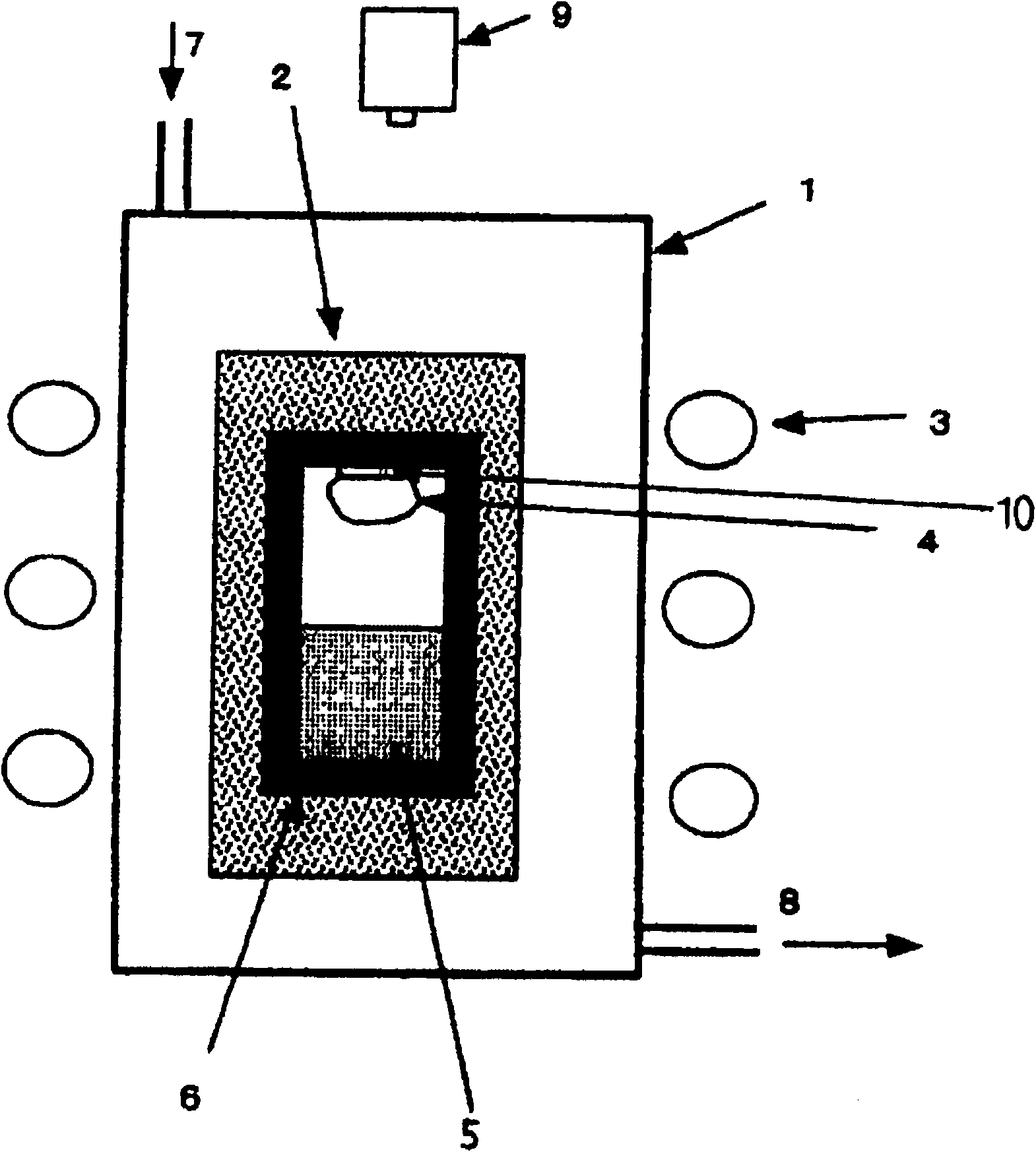
[0057] A graphite crucible with an inner diameter of 70 mm and a depth of 95 mm was filled with silicon carbide raw material powder (#240 manufactured by Showa Denko) to a height of 60 mm. Then un...


PUM

PropertyMeasurementUnit
thicknessaaaaaaaaaa
tensile strengthaaaaaaaaaa
thicknessaaaaaaaaaa

Abstract

A process for producing a single crystal of silicon carbide which comprises setting a low-temperature region and a high-temperature region in a crystal-growth crucible (6), disposing a seed-crystal substrate made of a single crystal of silicon carbide in the low-temperature region of the crystal-growth crucible, disposing raw silicon carbide in the high-temperature region, and precipitating a sublimation gas formed from the raw silicon carbide on the seed-crystal substrate to grow a single crystal of silicon carbide. In the process, the crucible member where the seed crystal is disposed is a member which differs from silicon carbide in the coefficient of room-temperature linear expansion by 1.0x10 / DEG K or less. Silicon carbide may be used as the crucible member where the seed crystal is disposed.

Description

technical field [0001] The invention relates to a method for manufacturing a silicon carbide single crystal. In particular, it relates to a method for producing a silicon carbide single crystal, characterized by using a crystal growth method for growing a high-quality silicon carbide single crystal. Background technique [0002] Silicon carbide is a material characterized by high thermal conductivity, excellent heat resistance and mechanical strength, strong resistance to radiation, etc., stable physical and chemical properties, and a wide bandwidth. Therefore, it can be used in environment-resistant element parts, radiation-resistant element parts, power supply element parts for electrical control, short-wavelength light-emitting element parts, and the like that can be used even at high temperatures. In addition, in recent years, it has attracted attention particularly as a power supply element for electric control, and extensive development has been carried out. [0003]...

Claims


Application Information

Patent Timeline
Patent Type & Authority Applications(China)
IPC IPC(8): C30B29/36C30B23/00
CPCC30B23/06C30B35/002C30B29/36C30B23/066
Inventor 庄内智博小古井久雄坂口泰之
Owner RESONAC CORP
Why Eureka
Try Eureka