Method for producing group iii nitride semiconductor layer, group iii nitride semiconductor light-emitting device, and lamp

A technology of nitride semiconductors and light-emitting elements, which is applied in the manufacture of semiconductor/solid-state devices, semiconductor devices, electrical components, etc., can solve problems such as residual damage to the light-emitting layer, load applied to the semiconductor layer, and defects in the light-emitting layer to prevent internal quantum efficiency. The reduction of the output power, the effect of reducing the leakage current

Inactive Publication Date: 2009-10-14
SHOWA DENKO KK
View PDF6 Cites 32 Cited by
  • Summary
  • Abstract
  • Description
  • Claims
  • Application Information

AI Technical Summary

Problems solved by technology

[0009] However, in a light-emitting element in which unevenness is formed on the light-extraction surface by mechanical processing or chemical processing, processing the light-extraction surface will apply a load to the semiconductor layer and leave damage to the light-emitting layer.
In addition, in a light-emitting element that grows a semiconductor layer under conditions such as forming unevenness on the light extraction surface, since the crystallinity of the semiconductor layer deteriorates, the light-emitting layer contains defects.
Therefore, when the light extraction surface is formed with irregularities, although the light extraction efficiency is improved, there is a problem that the internal quantum efficiency decreases and the luminous intensity cannot be increased.

Method used


Image

  • Method for producing group iii nitride semiconductor layer, group iii nitride semiconductor light-emitting device, and lamp
  • Method for producing group iii nitride semiconductor layer, group iii nitride semiconductor light-emitting device, and lamp
  • Method for producing group iii nitride semiconductor layer, group iii nitride semiconductor light-emitting device, and lamp

Examples


Embodiment 1

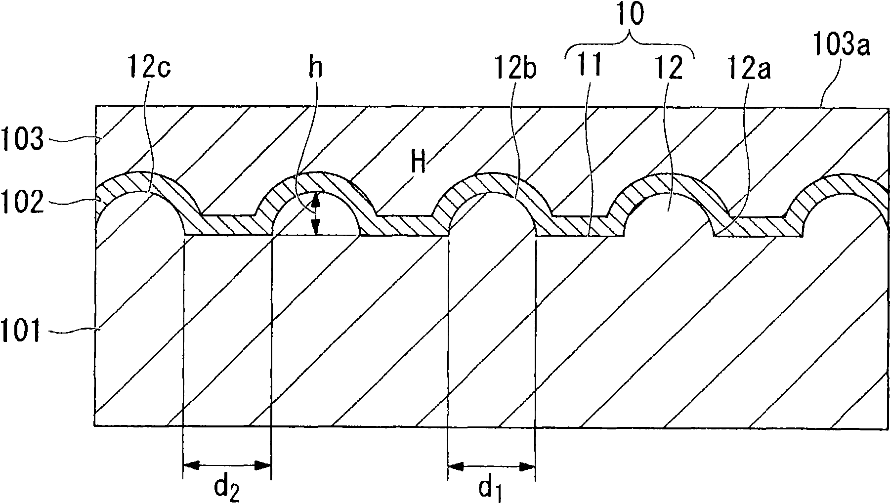
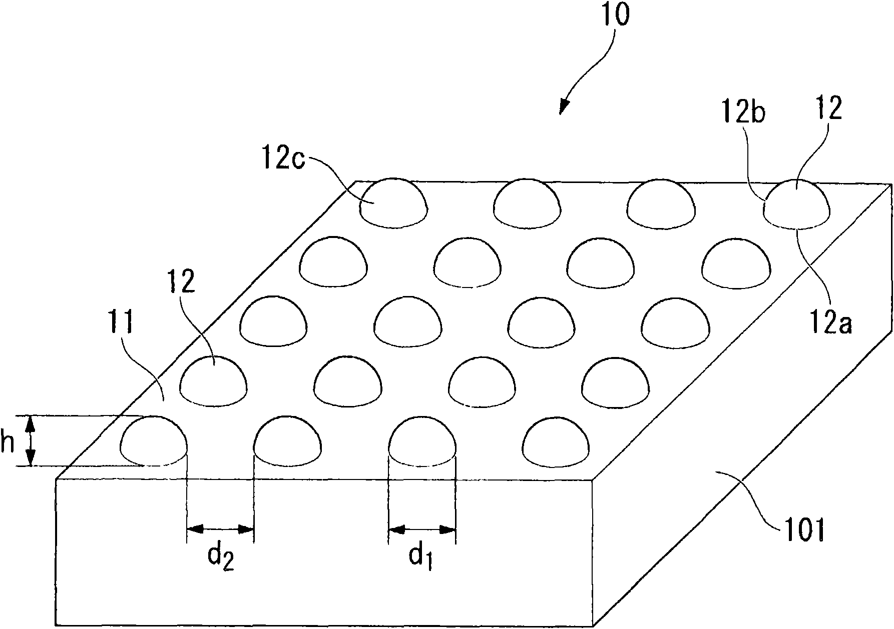
[0157] On the (0001) C plane of the sapphire substrate, the "base width", "height", "base width / 4", "interval between adjacent convex parts", "convex part width" shown in Table 1 are formed as follows. The presence or absence of multiple protrusions on the surface C surface (substrate processing process). That is, a mask was formed on a C-plane sapphire substrate with a diameter of 2 inches by a known photolithography method, and the convex portion was formed by etching the sapphire substrate by a dry etching method. In addition, as an exposure method, the step exposure method using ultraviolet rays was used. Also, using BCl in dry etching 3 with Cl 2 of the gas mixture.

[0158] Table 1

[0159]

[0160] The convex portion of Example 1 obtained in this way has a circular planar shape at the base, and a shape that gradually decreases toward the upper portion, and has a bowl-like (hemispherical) shape with sides curved outward.

Embodiment 2、 comparative example 4

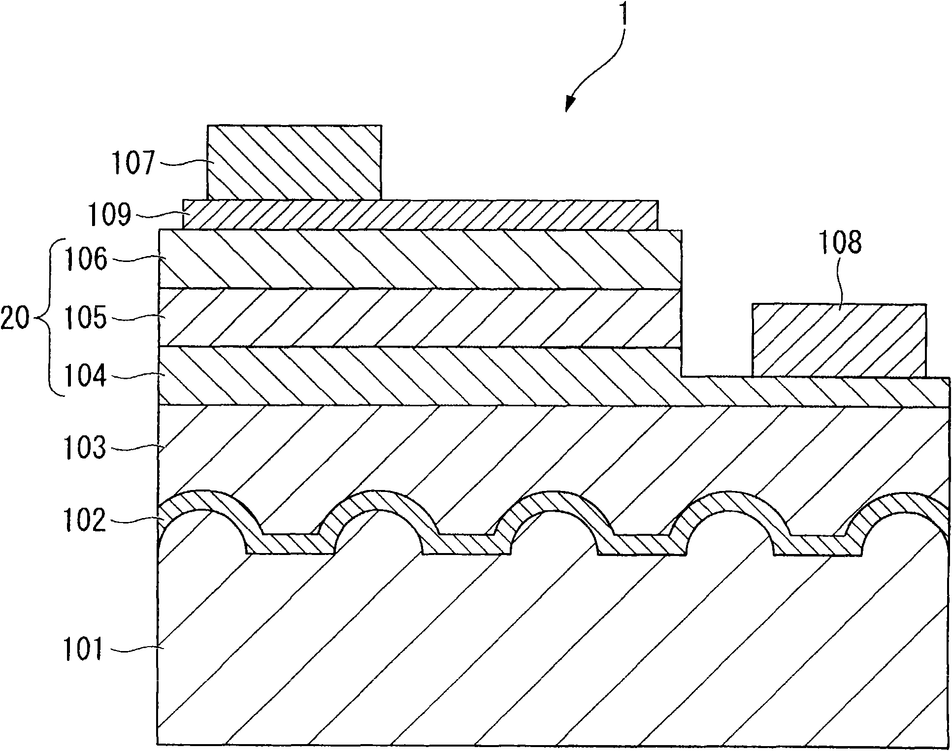
[0179] The n-type layer, the light-emitting layer, and the p-type layer forming the LED structure were stacked on the Group III nitride semiconductor layer prepared by the same method as in Example 1 and Comparative Example 3 by the method described below.

[0180] (n-type layer)

[0181] As the n-type layer, an n-contact layer and an n-cladding layer are formed. First, after growing the group III nitride semiconductor layer by the same method as in Example 1 and Comparative Example 3, the amount of ammonia was adjusted so that the ratio of group V (N) / group III (Ga) was 450, and the group III nitride semiconductor layer A 1 μm non-doped GaN layer is grown on it. Then under the same conditions, using monosilane (SiH 4 ) gas to form an n-contact layer composed of a 2 μm n-type GaN layer.

[0182] The doping amount of Si is 5×10 18 / cm 3 . After the n-contact layer was grown, the TMG valve was closed to stop the supply of TMG into the reaction furnace.

[0183] After the ...

Embodiment 3、 Embodiment 4、 comparative example 5

[0209] Embodiment 3, embodiment 4, comparative example 5, comparative example 6

[0210] In addition to the contents shown in Table 3, "base width", "height", "base width / 4", "interval between adjacent convex parts", and "presence of C surface on the surface of the convex part" were adopted and implemented. A light-emitting device was produced in the same manner as in Example 2 in the same manner as in Example 1 until the Group III nitride semiconductor layer was formed.

[0211] In addition, the convex part of Example 3, Example 4, and Comparative Example 6 has a circular planar shape of the base, a shape that gradually becomes smaller toward the upper part, and a bowl-shaped shape with sides curved outward. In addition, the protrusions of Example 3, Example 4, and Comparative Example 6 are protrusions obtained by changing the height of the protrusions by changing the etching time.

[0212] Then, a current of 20 mA was applied in the forward direction to the obtained light-e...


PUM

PropertyMeasurementUnit
heightaaaaaaaaaa
thicknessaaaaaaaaaa
thicknessaaaaaaaaaa

Abstract

Disclosed is a method for producing a group III nitride semiconductor layer having excellent crystallinity which can be suitably used for forming a light-emitting device having excellent internal quantum efficiency and light extraction efficiency. Specifically disclosed is a method for producing a single crystal group III nitride semiconductor layer (103) on a substrate (101), which comprises a substrate processing step wherein a plurality of projected portions (12) composed of surfaces 12c not parallel to (0001)C-plane of the substrate (101) are formed on the (0001)C-plane, thereby forming an upper surface (10) composed of a flat surface (11) composed of the(0001)C-plane and the projected portions (12); and an epitaxial step for epitaxially growing the group III nitride semiconductor layer (103) on the upper surface (10), thereby embedding the projected portions (12) in the group III nitride semiconductor layer (103).

Description

technical field [0001] The present invention relates to a method for producing a group III nitride semiconductor layer suitably used for a light emitting device such as a light emitting diode (LED), and to a group III nitride semiconductor light emitting device and a lamp. [0002] This application is based on patent application No. 2006-346000 filed in Japan on December 22, 2006, patent application No. 2007-224496 filed in Japan on August 30, 2007, and patent application No. 2007-224496 filed in Japan on October 22, 2007 Patent application No. 2007-274376 and patent application No. 2007-286690 filed in Japan on November 2, 2007 claim priority only, and the contents thereof are incorporated herein. Background technique [0003] In recent years, Group III nitride semiconductors have attracted attention as semiconductor materials for light-emitting devices that emit short-wavelength light. Group III nitride semiconductors are composed of the general formula Al x Ga y In z ...

Claims


Application Information

Patent Timeline
Patent Type & Authority Applications(China)
IPC IPC(8): H01L33/00H01L21/205
Inventor 篠原裕直酒井浩光
Owner SHOWA DENKO KK
Why Eureka
Try Eureka