Photoelectric packaging part with cavity and production method thereof

A packaging and optoelectronic technology, applied in electrical components, electric solid-state devices, semiconductor devices, etc., can solve the problems of affecting the packaging yield rate of the whole machine installation qualification rate, affecting the high-frequency performance of the circuit, reducing the material utilization rate, etc. The effect of high packaging yield, high production efficiency and high pass rate

Active Publication Date: 2009-10-21
TIANSHUI HUATIAN TECH
View PDF0 Cites 17 Cited by
  • Summary
  • Abstract
  • Description
  • Claims
  • Application Information

AI Technical Summary

Problems solved by technology

[0005] 1. The packaged product has exposed gull-wing-shaped outer pins, which are easily damaged and deformed during production, transportation, and use, resulting in poor coplanarity and affecting the packaging yield and the overall installation pass rate;
[0006] 2. Because the product has long external pins, the lead capacitance is large, which

Method used


Image

  • Photoelectric packaging part with cavity and production method thereof
  • Photoelectric packaging part with cavity and production method thereof
  • Photoelectric packaging part with cavity and production method thereof

Examples


Embodiment 1

[0059] 1. Production of plastic-encapsulated outer cavity

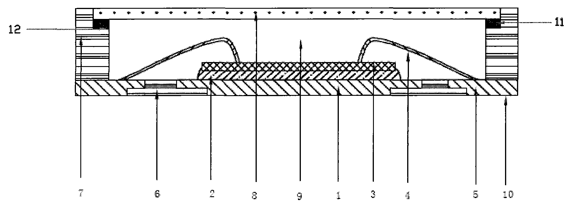
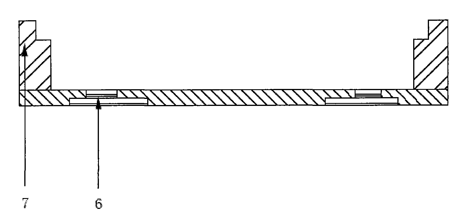
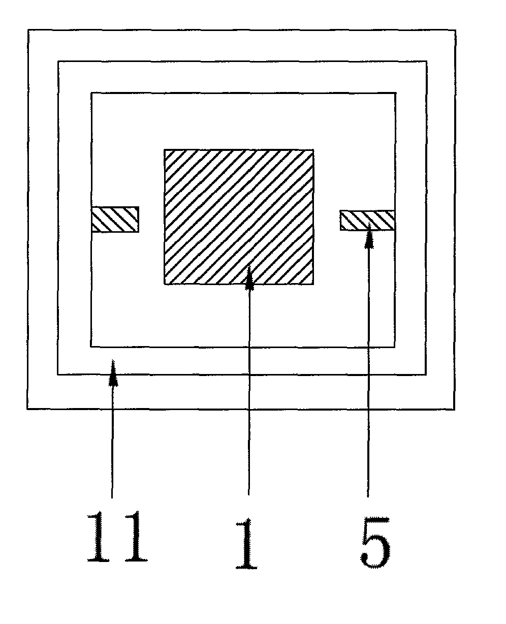
[0060] A plastic encapsulation system is used to automatically transfer the lead frame into a plastic encapsulation mold, and a cavity with a height of 0.5 mm with a step is formed above the outer pins of the lead frame through plastic encapsulation, and the cavity covers the outer pins of the lead frame. The side of the lead frame carrier 1 and the space on the side of the pin 5 in the lead frame are connected by the plastic package 6, and the lower surface of the plastic package 6, the lead frame carrier (base island, PAD) 1 and the bottom surface of the outer pins of the lead frame are in the same position. a plane. Send the semi-finished product with the cavity ready for curing, and cure according to the conventional curing process after plastic sealing.

[0061] 2. Wafer thinning / scribing

[0062] First paste the adhesive film on the front, and then thin it on a special thinning machine to meet the process requ...

Embodiment 2

[0078] 1. Production of plastic-encapsulated outer cavity

[0079] A plastic encapsulation system is used to automatically transfer the lead frame into a plastic encapsulation mold, and a cavity with a height of 0.7 mm with a step is formed above the outer pins of the lead frame through plastic encapsulation, and the cavity covers the outer pins of the lead frame. The side of the lead frame carrier 1 and the space on the side of the pin 5 in the lead frame are connected by the plastic package 6, and the lower surface of the plastic package 6, the lead frame carrier (base island, PAD) 1 and the bottom surface of the outer pins of the lead frame are in the same position. a plane. Send the semi-finished product with the cavity ready for curing, and cure according to the conventional curing process after plastic sealing.

[0080] 2. Wafer thinning / scribing

[0081] First paste the adhesive film on the front, and then thin it on a special thinning machine to meet the process requ...

Embodiment 3

[0097] The overall process steps are the same as in Example 1 or 2, only in step 4 bonding, the time of ultrasonic wave and pressure added to the wiring rivet is 13ms, the ultrasonic frequency is 130KHZ, the output mode is current, the power is 44mw; the pressure output is 34gf ;

[0098] Step 6. The baking time during curing is as follows: heating time is 25 minutes, constant temperature time is 75 minutes, and cooling time is 35 minutes.


PUM


Abstract

The invention provides a photoelectric packaging part with a cavity. An annular outer cavity with inner steps is arranged on a lead frame outer pin by a plastic packaging die, and a plastic packaging outer cavity covers the lead frame outer pin; and gap between an inner pin and a lead frame carrier is connected by a plastic packaging body to form the whole circuit. The production method comprises the following steps: making the plastic packaging outer cavity; thinning down and scribing silicon wafer; molding core; bonding; cementing a glass cover plate; curing; electroplating; printing; and cutting, separating and feeding. The photoelectric packaging part is characterized by simple structure, no exposed outer pin, no coplanarity defect, high chip packaging yield and high installation qualification rate of finished devices. The adopted production method has the advantages of no dambar and forming process, high utilization rate of materials, the adopted glass cover plate made from low-temperature glass and other materials, and higher production efficiency, which is beneficial to product installation. The photoelectric packaging part has the advantages of low cost, small size, high sensitivity, low power consumption, strong anti-interference capacity and good reliability.

Description

technical field [0001] The invention relates to the technical field of electronic information automation component manufacturing, in particular to an optoelectronic chip integrated circuit package, specifically a cavity-equipped optoelectronic integrated circuit package, and the invention includes a production method of the package. Background technique [0002] At present, the general optoelectronic package is packaged in DIP or QFP ceramic inner cavity. Its structure is that the circuit pins are on the outside of the package, and there is a square gold-plated substrate at the bottom of the inner cavity of the package. On the substrate is an adhesive ( Conductive glue or insulating glue), the adhesive glue is IC or photoelectric chip, the pad (PAD) on the IC or photoelectric chip is bonded to the first step on the inner cavity by gold wire (silicon aluminum wire, copper wire) The gold-plated inner lead pins are connected to form the signal and power channels of the circuit....

Claims


Application Information

Patent Timeline
IPC IPC(8): H01L27/144H01L27/146H01L23/02H01L23/04H01L23/10H01L23/495H01L21/50H01L21/52H01L21/607
CPCH01L2924/10253H01L2224/48091H01L2224/73265H01L2224/45147H01L2224/45124H01L2224/45144H01L2924/01047
Inventor 慕蔚
Owner TIANSHUI HUATIAN TECH
Why Eureka
Try Eureka