Surface-texturing n-type ZnO-based transparent conductive film and preparation method thereof

A technology of transparent conductive film and surface texture, applied in circuits, photovoltaic power generation, electrical components, etc., can solve the problems of damage, complex processing procedures, and difficulty in large-scale production.

Active Publication Date: 2009-10-28
SHANGHAI INST OF CERAMIC CHEM & TECH CHINESE ACAD OF SCI
View PDF0 Cites 24 Cited by
  • Summary
  • Abstract
  • Description
  • Claims
  • Application Information

AI Technical Summary

Problems solved by technology

Whether it is the wet chemical method of dilute acid surface etching or the dry etching method of plasma, it is necessary to prepare a transparent conductive film first and then perform surface treatment. The treatment process is complicated, and the uniformity and repeatability are poor.
In addition, the wet surface corrosion reaction will also cause certain damage to the internal structure of the film, causing more defects such as grain boundaries and dislocations to appear in the film, and the mechanical strength of the film will decrease, thereby affecting the performance of the solar cell; and the plasma Dry etching also has problems such as complex process and high cost, making it difficult to apply to large-scale production

Method used


Image

  • Surface-texturing n-type ZnO-based transparent conductive film and preparation method thereof
  • Surface-texturing n-type ZnO-based transparent conductive film and preparation method thereof
  • Surface-texturing n-type ZnO-based transparent conductive film and preparation method thereof

Examples


Embodiment 1

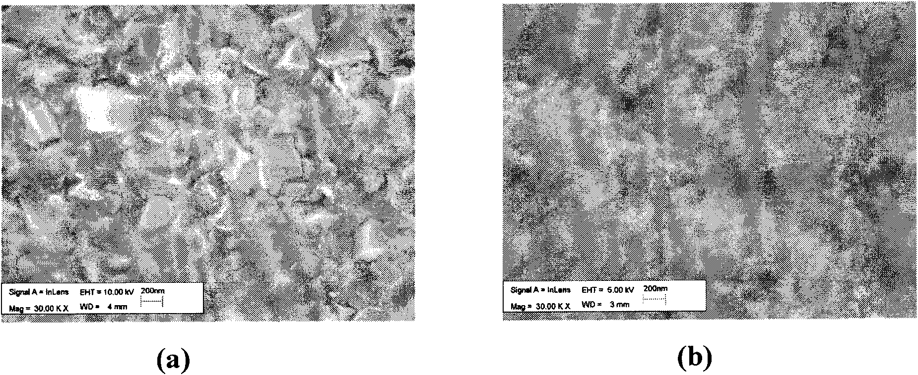
[0034] ZnO-based doping compound (ZnO:Al) is used as the target material, the doping ratio of Al is 2.0mol%, and ordinary glass is used as the substrate, and the background vacuum is pumped to 2.0×10 -4 Pa, with high-purity argon as the working gas, and a small amount of O 2 and H 2 Gas (O 2 and H 2 accounted for 5% and 2% of the total gas flow respectively), the working pressure was maintained at 1.2Pa, the substrate temperature was 150°C, the distance between the target and the substrate was set at 7cm, DC magnetron sputtering was adopted, and the sputtering power was 80W. The deposition time is 40min. The surface morphology of the prepared film samples is as follows figure 1 (a) shown. The results show that the AZO film prepared by the invention has good crystallization, large grain size, and obvious grain boundaries between grains.

Embodiment 2

[0036] ZnO-based doping compound (ZnO:Al) is used as the target material, the doping ratio of Al is 2.0mol%, and ordinary glass is used as the substrate, and the background vacuum is pumped to 2.0×10 -4 Pa, using high-purity argon as the working gas, the working pressure is maintained at 1.2Pa, the substrate temperature is 150°C, the distance between the target and the substrate is set at 7cm, DC magnetron sputtering is used, the sputtering power is 80W, the deposition time for 40min. Using pure Ar gas as the working gas, under the same process conditions, the surface morphology of the obtained film is as follows: figure 1 (b). Obviously, there is no 2 and H 2 When the gas is fed, the grain boundaries of the AZO film are relatively disordered, and the grain size is small; while in Example 1, a small amount of O 2 and H 2 After being degassed, Al atoms are effectively incorporated into the ZnO lattice instead of at the grain boundaries, the grains grow significantly, and t...

Embodiment 3

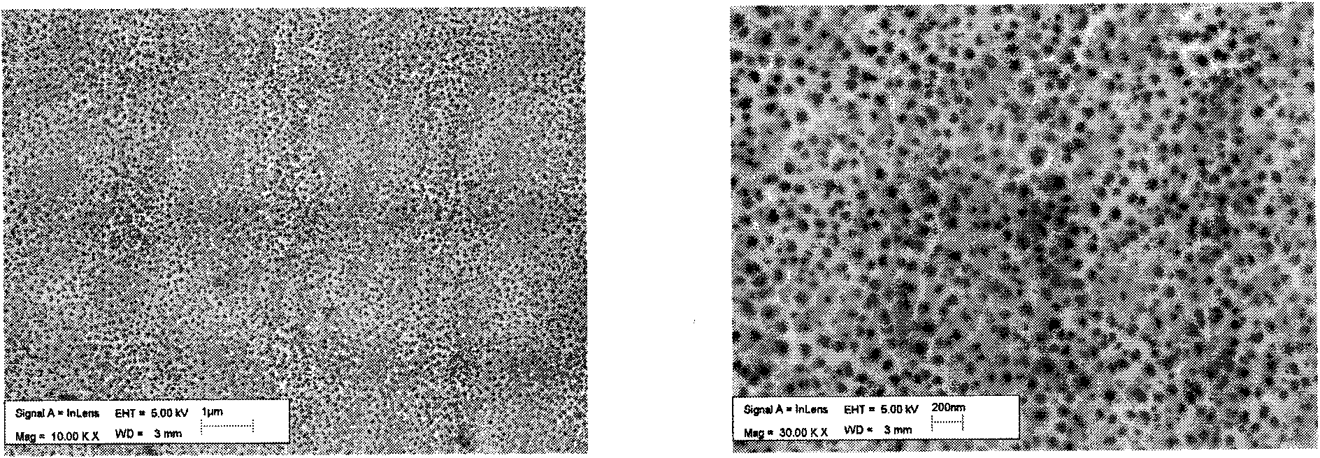
[0038] ZnO-based doping compound (ZnO:Al) is used as the target material, the doping ratio of Al is 2.0mol%, and ordinary glass is used as the substrate, and the background vacuum is pumped to 2.0×10 -4 Pa, with high-purity argon as the working gas, and a small amount of O 2 and H 2 Gas (O 2 and H 2 accounted for 5% and 2% of the total gas flow respectively), the working pressure was maintained at 1.2Pa, the substrate temperature was 90°C, the distance between the target and the substrate was set at 7cm, DC magnetron sputtering was adopted, and the sputtering power was 80W. The deposition time is 40min. Next, adjust O 2 and H 2 Gas volume (O 2 and H 2 accounted for 0.05% and 5.0% of the total gas flow respectively), the working pressure was maintained at 0.3Pa, the substrate temperature was room temperature, the distance between the target and the substrate was set at 5cm, DC magnetron sputtering was adopted, and the sputtering power was 140W. The time is 10 minutes. ...


PUM

PropertyMeasurementUnit
electrical resistivityaaaaaaaaaa

Abstract

The invention relates to a surface-texturing n-type ZnO-based transparent conductive film and a preparation method thereof. The invention forms a large amount of microporous structures with regular arrangement, uniform structure, good communication and a certain depth on the film surface of the conductive film. The surface-texturing film has excellent light capture performance and extremely high conductivity simultaneously. The surface-texturing n-type ZnO-based transparent conductive film prepared by direct current magnetic control continuous sputtering has simple process and easily monitored quality, is suitable for large-scale production, can keep excellent column-shaped crystal structure of the body film, has complete communication between holes and keeps high conductivity of the ZnO-based film; the micropore on the texture surface has excellent uniformity and repeatability compared to the two traditional methods; furthermore, the depth and the diameter of the hole are controllable within a certain range; the average transmissivity of the film layer at the visible light area reaches more than 90%, the mobility is up to 35.4cm[2]/V.S, the resistivity is 1.003*10[-4]Omega.cm and the sheet resistance reaches 0.9 Omega.

Description

technical field [0001] The invention relates to a surface textured n-type ZnO-based transparent conductive film and a preparation method thereof, belonging to the technical field of transparent conductive material (TCM) films. Background technique [0002] Since the first translucent conductive CdO material [K. Badeker, Ann. Phys. Leipzig, 1907, 22, 749] came out in 1907, due to the needs of industrial energy, transparent conductive materials have received unprecedented attention and wide application. Taking 2004 as an example, the transaction volume of the flat-panel display market related to transparent conductors was about 25 billion US dollars. It can be seen that the importance of transparent conductor materials is extraordinary [D.S.Ginley, C.Bright, eds., MRS Bulletin, 2000, 25, 15]. Transparent conductive materials are required to have high transparency and high conductivity which are almost incompatible with each other. At present, most of the main transparent con...

Claims


Application Information

Patent Timeline
Patent Type & Authority Applications(China)
IPC IPC(8): H01L31/0224H01L31/0236H01L31/18C23C14/34
CPCY02E10/50Y02P70/50
Inventor 万冬云黄富强
Owner SHANGHAI INST OF CERAMIC CHEM & TECH CHINESE ACAD OF SCI
Why Eureka
Try Eureka