

Inner cavity type multiple-active region photon crystal vertical cavity surface transmission semiconductor laser device
A vertical cavity surface emission, photonic crystal technology, applied in the field of optoelectronics, can solve the problems of difficult control of small oxide holes, poor thermal stability of devices, low single-mode output power, etc., to achieve narrow line width and improve thermal stability. , emphasize the effect of the control feature
- Summary
- Abstract
- Description
- Claims
- Application Information
AI Technical Summary
Problems solved by technology
Method used
Image

Examples
Embodiment Construction
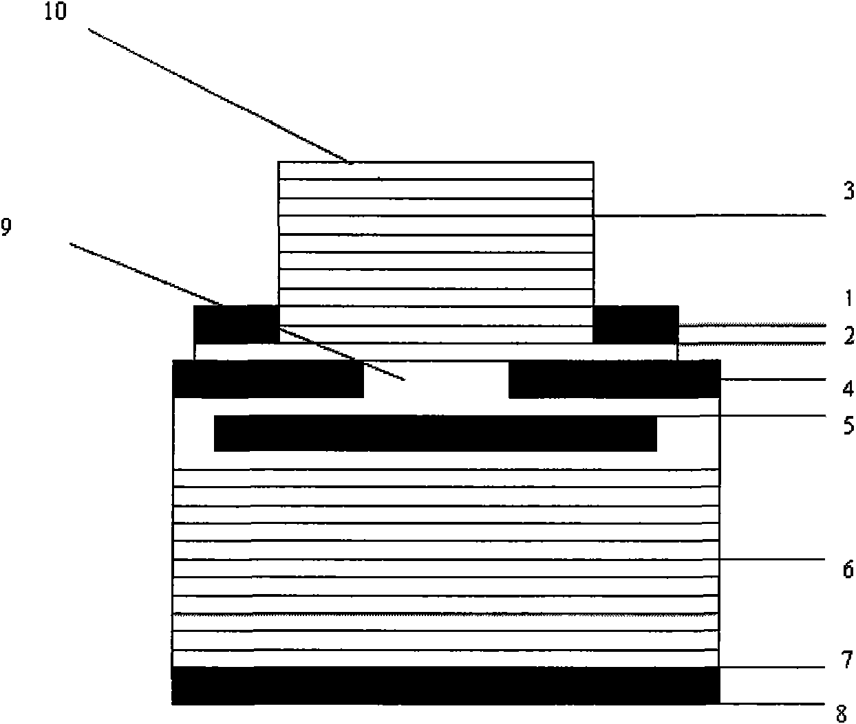
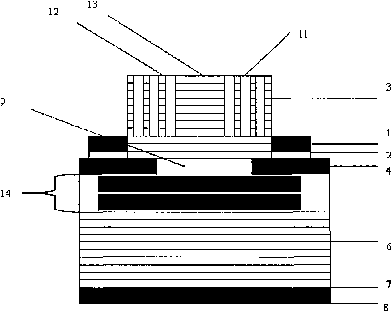
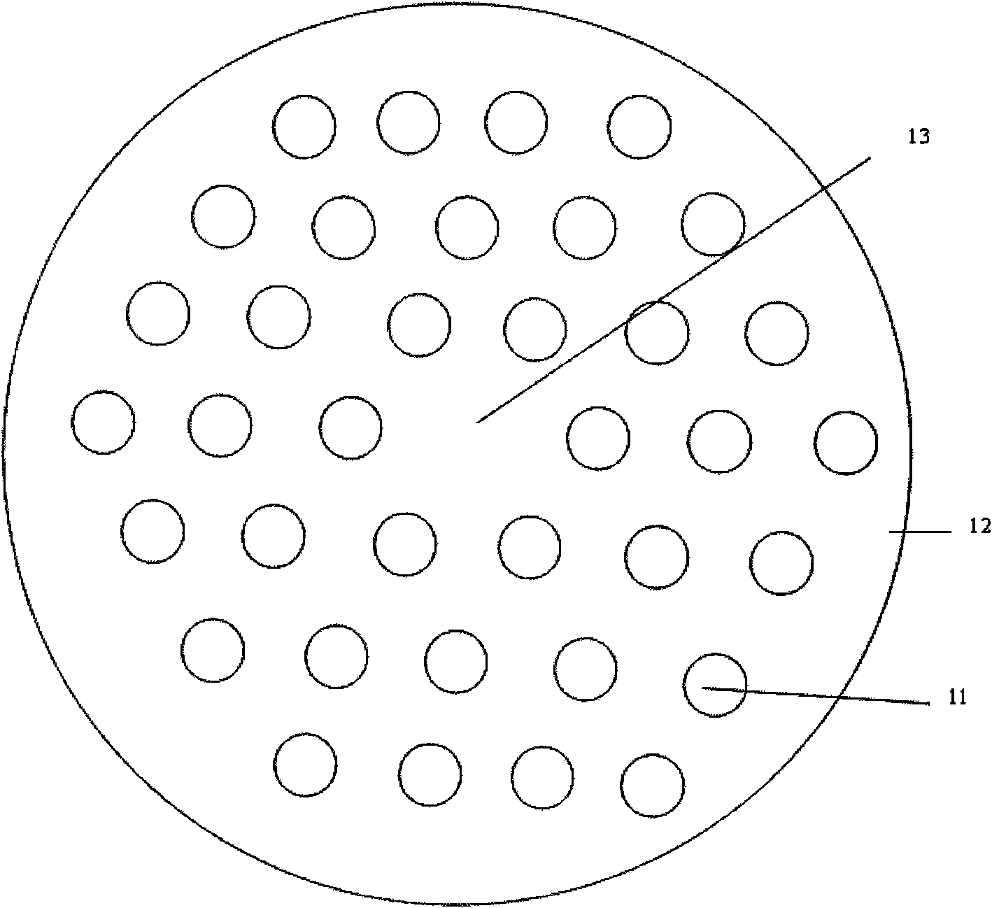
[0032] (Take the wavelength 850nm as an example)
[0033] 1. Pass in N + The substrate 7 was obtained by growing on a GaAs substrate of type 1, and then a 0.3 micron GaAs buffer layer was grown on the substrate by MOCVD method, and then N + al 0.1 Ga 0.9 As (60nm doping concentration 3×10 18 cm -3 ) and n + al 0.9 Ga 0.1 As (68.19nm doping concentration 3×10 17 cm -3 ) composed of 28 cycles of the lower DBR6, In 0.18 al 0.12 Ga 0.7 As and Al 0.22 Ga 0.78 AS composed of single active region 5 heavily doped N + GaAs and P + Multiple active regions (three active regions) cascaded with GaAs reverse tunnel junctions 14, Al 0.98 Ga 0.02 As (30nm doping concentration 1×10 18 cm -3 ) oxidation limiting layer 4, Al 0.1 Ga 0.9 As heavily doped ohmic contact layer 2, undoped Al 0.1 Ga 0.9 As(60nm) and Al 0.9 Ga 0.1 24-period upper DBR3 composed of As (68.19nm).
[0034] 2. Using the traditional oxidation-limited vertical cavity surface-emitting semiconductor las...
PUM
 Abstract
Description
Claims
Application Information