

Method for manufacturing micropores for electric conduction among copper foil of high-density multilayer circuit boards
A multi-layer circuit board and manufacturing method technology, applied in the direction of electrical connection formation of printed components, etc., can solve the problems of large discharge of organic and acidic pollutants, low production efficiency, high cost of Excimer lasers, etc.
- Summary
- Abstract
- Description
- Claims
- Application Information
AI Technical Summary
Problems solved by technology
Method used
Image

Examples
Embodiment 1
[0034] The micropore manufacturing method of the present embodiment is carried out according to the following steps:
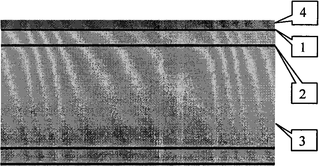
[0035] (1) First paste a layer of insulating tape 4 on the surface copper foil 1 of the high-density multilayer circuit board (such as figure 2 );
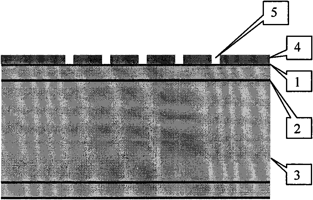
[0036] (2) Use 20J / cm 2 Density pulsed carbon dioxide laser micro-beams ablate the insulating tape 4 at the microhole to be drilled to form the microhole 5 of the insulating tape, so that the surface copper foil 1 at the microhole to be drilled is exposed (such as image 3 );
[0037] (3) electroplating a layer of tin-containing metal layer 6 with a thickness of 4.5 microns (such as Figure 4 ), the tin-containing metal layer 6 is partially electroplated with a tin-silver alloy;
[0038] (4) peel off the insulating tape 4 pasted on the surface copper foil 1, and only have the tin-containing metal layer 6 at the microhole to be drilled on the surface of the copper foil (such as Figure 5 ).
[0039] (5) Use ...
Embodiment 2
[0042] The micropore manufacturing method of the present embodiment is carried out according to the following steps:
[0043] (1) First paste a layer of insulating tape 4 on the surface copper foil 1 of the high-density multilayer circuit board (such as figure 2 );
[0044] (2) Use 20J / cm 2 Density pulsed carbon dioxide laser micro-beams ablate the insulating tape 4 at the microhole to be drilled to form the microhole 5 of the insulating tape, so that the surface copper foil 1 at the microhole to be drilled is exposed (such as image 3 );
[0045] (3) Electroplating a layer of pure tin metal layer 6 with a thickness of 5.0 microns on the surface copper foil 1 exposed to the micro-hole to be drilled, the pure tin metal layer 6 adopts a partial electroplating method; the electroplating solution adopts commercially available tin electroplating solution, the electroplating process conditions are as follows:
[0046] Composition Rack Plating
[0047] SnSO 4 40 g / l...
Embodiment 3
[0059] The micropore manufacturing method of the present embodiment is carried out according to the following steps:
[0060] (1) First paste a layer of insulating tape 4 on the surface copper foil 1 of the high-density multilayer circuit board (such as figure 2 );
[0061] (2) Use 20J / cm 2 Density pulsed carbon dioxide laser micro-beams ablate the insulating tape 4 at the microhole to be drilled to form the microhole 5 of the insulating tape, so that the surface copper foil 1 at the microhole to be drilled is exposed (such as image 3 );
[0062] (3) Electroplating a layer of pure tin metal layer 6 with a thickness of 5.0 microns on the surface copper foil 1 exposed to the micro-hole to be drilled, the pure tin metal layer 6 adopts a partial electroplating method; the electroplating solution adopts commercially available tin electroplating solution, the electroplating process conditions are as follows:
[0063] Composition Rack Plating
[0064] SnSO 4 40 g...
PUM
| Property | Measurement | Unit |
|---|---|---|
| Thickness | aaaaa | aaaaa |
| Thickness | aaaaa | aaaaa |
Abstract
Description
Claims
Application Information