Transition layer film with Gd mixed with CeO<2> and preparation method thereof

A transition layer and thin film technology, applied in the field of high temperature superconducting material preparation, achieves the effects of flat and compact surface, simple preparation process and long service life

Inactive Publication Date: 2011-11-16
BEIJING UNIV OF TECH
View PDF0 Cites 2 Cited by
  • Summary
  • Abstract
  • Description
  • Claims
  • Application Information

AI Technical Summary

Problems solved by technology

[0005] The purpose of the present invention is to solve the problems existing in the preparation process of the existing coating conductor transition layer, and to provide a simple, efficient, and low-cost Gd-doped CeO 2 Single transition layer thin film and preparation method thereof

Method used


Image

  • Transition layer film with Gd mixed with CeO&lt;2&gt; and preparation method thereof
  • Transition layer film with Gd mixed with CeO&lt;2&gt; and preparation method thereof
  • Transition layer film with Gd mixed with CeO&lt;2&gt; and preparation method thereof

Examples


Embodiment 1

[0028] 1) adding cerium acetate and gadolinium acetate into n-propionic acid, heating and stirring until dissolved, according to the molar ratio of cerium ion and gadolinium ion being 0.9:0.1, and the total concentration of cerium ion and gadolinium ion being 0.1mol / L, to obtain a precursor solution;

[0029] 2) Coating the precursor solution onto the NiW metal base tape by spin coating, the rotation speed is 2000rpm, and the time is 30s to obtain the precursor film;

[0030] 3) in H 2 Under gas protection conditions, the precursor film was sintered at 950 °C for 120 minutes to obtain a 30 nm thick Ce with cubic texture 0.9 Gd 0.1 o 2 Single transition layer film.

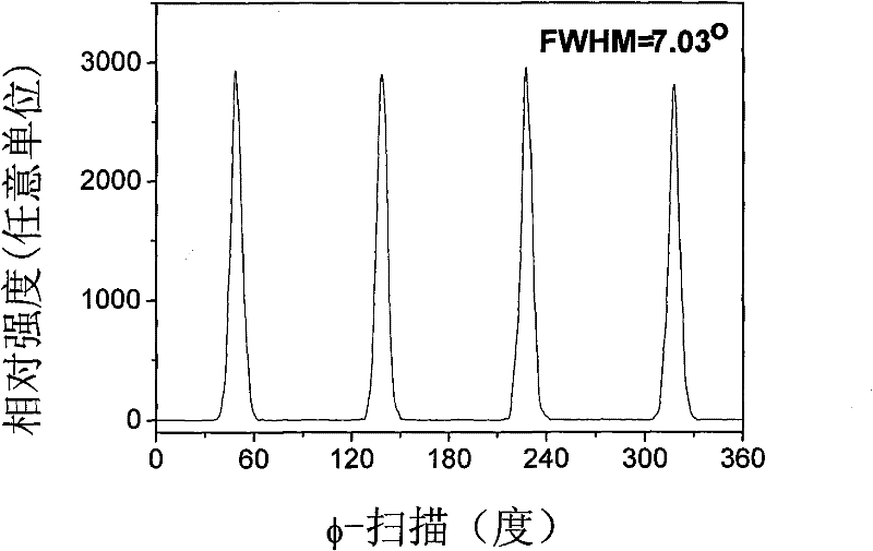
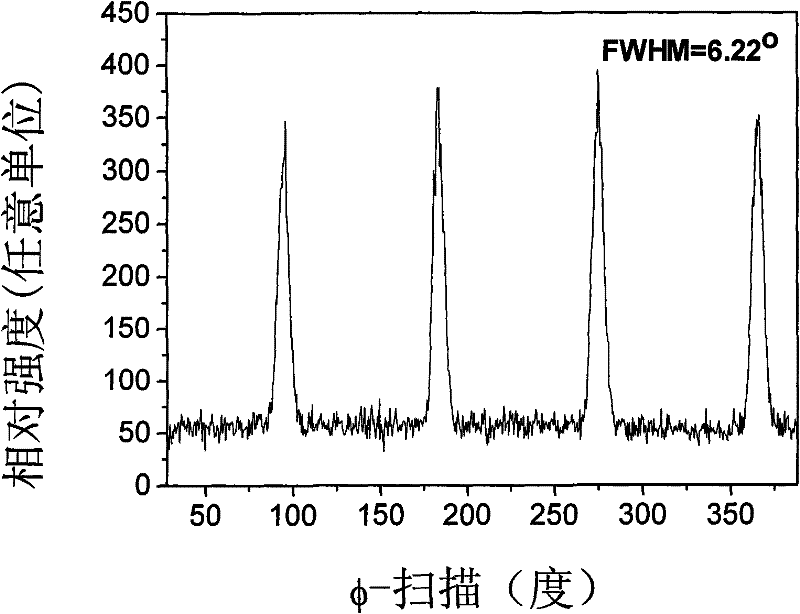
[0031] figure 1 It is the phi scanning diagram of the NiW alloy substrate (111) surface used, figure 2 for Ce 0.9 Gd 0.1 o 2 The (111) plane phi scan of the transition layer film has a FWHM (width at half maximum) of 6.22, which is 0.81 smaller than that of the NiW baseband, indicating that the Ce 0.9 Gd ...

Embodiment 2

[0033] 1) Add cerium acetate and gadolinium acetate to n-propionic acid, heat and stir until dissolved, according to the molar ratio of cerium ion to gadolinium ion is 0.8:0.2, and the total concentration of cerium ion and gadolinium ion is 0.4mol / L, to obtain a precursor solution ;

[0034] 2) Coating the precursor solution onto the NiW metal base tape by spin coating, the rotation speed is 5000rpm, and the time is 120s to obtain the precursor film;

[0035] 3) in H 2 Mixing with Ar (H 2 The volume percentages of Ar and Ar are 5% and 95%, respectively) under gas protection conditions, the precursor film was sintered at 1200 ° C for 15 minutes to obtain a 60nm thick Ce with cubic texture 0.8 Gd 0.2 o 2 Single transition layer film.

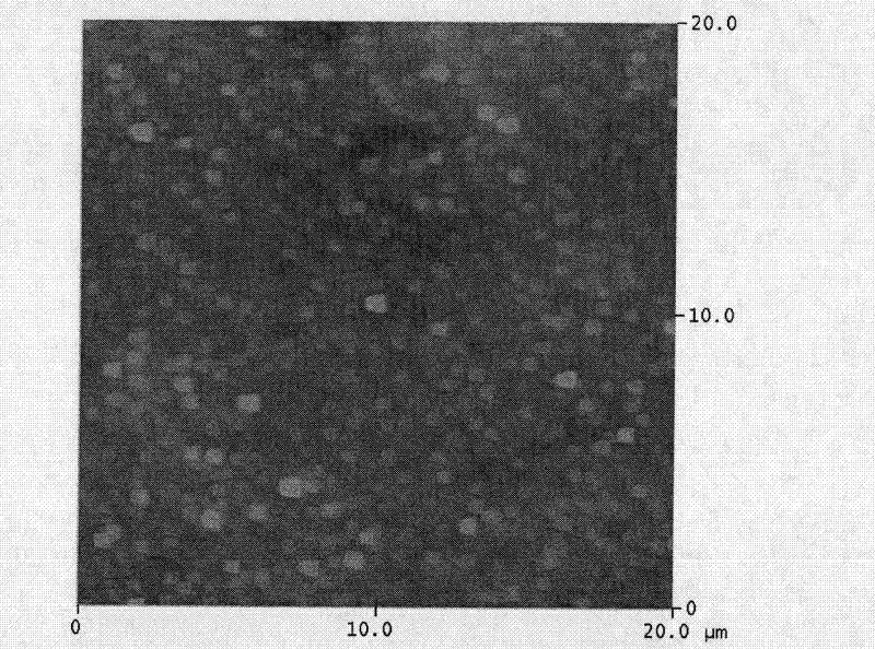
[0036] Ce 0.8 Gd 0.2 o 2 The surface morphology of the single-layer transition layer film is as follows: image 3 It can be seen from the AFM photo that the surface of the transition layer is flat and dense, the grains are fine and unifor...

Embodiment 3

[0038] 1) Add cerium acetate and gadolinium acetate to n-propionic acid, heat and stir until dissolved, at a molar ratio of cerium ions to gadolinium ions of 0.5:0.5, and a total concentration of cerium ions and gadolinium ions of 0.3 mol / L, to obtain a precursor solution ;

[0039]2) Coating the precursor solution onto the NiW metal substrate by dipping method, pulling the NiW metal substrate at a speed of 150 mm / min to obtain a precursor film;

[0040] 3) in N 2 Under gas protection conditions, the precursor film was sintered at 1150 °C for 60 minutes to obtain a 50 nm thick Ce with cubic texture 0.5 Gd 0.5 o 2 Single-layer transition layer film;

[0041] 4) Multi-layer coating: repeat steps 2) and 3) 4 times to obtain a Ce with a thickness of 250nm 0.5 Gd 0.5 o 2 5-layer transition layer film.

[0042] Ce 0.5 Gd 0.5 o 2 The XRD pattern of the five-layer transition layer film is as follows Figure 4 It can be seen from the figure that no impurity phase is formed ...


PUM

PropertyMeasurementUnit
thicknessaaaaaaaaaa
thicknessaaaaaaaaaa
thicknessaaaaaaaaaa

Abstract

The present invention relates to a transition layer film with Gd mixed with CeO2 and a preparation method thereof, belonging to the technical field of high temperature superconduction material preparation. The transition layer film with Gd mixed with CeO2 provided by the invention consists of Ce1-xGdxO2 composite oxide sosoloid, wherein, x is more than or equal to 0.1 and less than or equal to 0.5; and the thickness of the transition layer film is 30-250nm. The invention takes cerium acetate as precursor and gadolinium acetate as gadolinium source, uses chemical solution method to prepare precursor solution, coats the precursor solution on metal base bands by a spin coating or dip coating method, and prepares the transition layer film with Gd mixed with CeO2 by thermal treatment process. The transition layer film with Gd mixed with CeO2 and the preparation method thereof provided by the present invention has the advantages of simple preparation process, low cost, large thickness but no crack of the film, level, even and compact surface of the texture through which the film is capable of extending the base of the film, the role in separating mutual reaction between the superconduction layer and the base material, etc.

Description

technical field [0001] The invention belongs to the technical field of high-temperature superconducting material preparation, and in particular relates to the preparation technology of a high-temperature superconducting coating conductor transition layer. Background technique [0002] The second-generation coated superconductor of rare earth barium copper oxide mainly based on YBCO, due to its high irreversible field, high current carrying capacity, low AC loss, and potential price advantage, was recognized as early as the end of the 1980s. The prediction will have a very broad application prospect. However, due to the intrinsic characteristics of the YBCO material: sufficient oxygen needs to be introduced during the preparation process to convert it into a superconducting phase; the critical current density strongly depends on the angle between the grain boundaries; chemical reactions with most metal materials will occur, resulting in its very It is difficult to prepare hi...

Claims


Application Information

Patent Timeline
Patent Type & Authority Patents(China)
IPC IPC(8): C04B35/50C04B35/622
Inventor 刘敏索红莉叶帅赵跃马麟程艳玲王榕吕昭周美玲
Owner BEIJING UNIV OF TECH
Why Eureka
Try Eureka