Method for testing polarity of semiconductor crystal or epitaxial thin film material and test system

A technology for epitaxial thin films and semiconductors, which is applied in the fields of analyzing materials, using wave/particle radiation for material analysis, and measuring devices, etc. It can solve the problems of demanding sample surface cleanliness, difficulty in sample preparation and instrument operation, and low accuracy. To achieve the effect of simple and fast sample preparation, lower test costs, and easy operation

Inactive Publication Date: 2009-12-30
东莞燕园半导体科技有限公司
View PDF0 Cites 12 Cited by
  • Summary
  • Abstract
  • Description
  • Claims
  • Application Information

AI Technical Summary

Problems solved by technology

The most commonly used methods are converged beam electron diffraction and chemical corrosion. The former needs to be measured simultaneously with the transmission electron microscope. Not only is the instrument expensive, sample preparation and instrument operation are difficult, it is destructive to the sample, and it cannot be judged on a large scale.
Although the method of chemical corrosion is relatively simple, its accuracy is poor and it is also destructive to the sample
Although the two methods of X-ray photoelectron spectroscopy and coaxial ion scattering are not destructive to the sample, the test requires an ultra-high vacuum system and has strict requirements on the cleanliness of the sample surface. In addition, the results need to be simulated with the theoretical calculation results. Large volume and low precision

Method used


Image

  • Method for testing polarity of semiconductor crystal or epitaxial thin film material and test system
  • Method for testing polarity of semiconductor crystal or epitaxial thin film material and test system
  • Method for testing polarity of semiconductor crystal or epitaxial thin film material and test system

Examples


Embodiment Construction

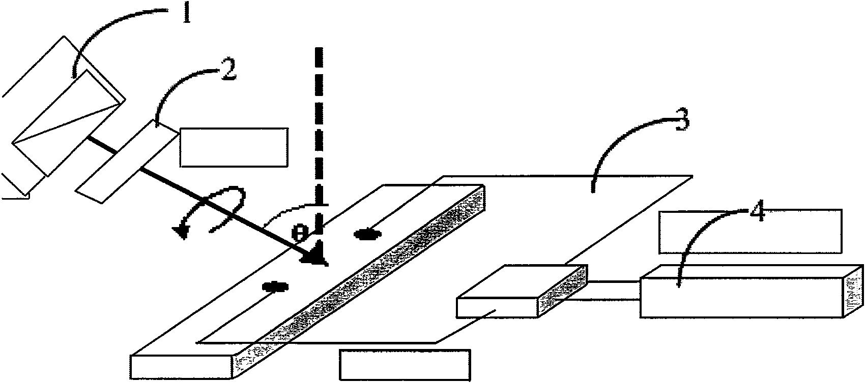
[0018] The specific implementation manners of the present invention will be further described in detail below in conjunction with the accompanying drawings and embodiments. The following examples are used to illustrate the present invention, but are not intended to limit the scope of the present invention.

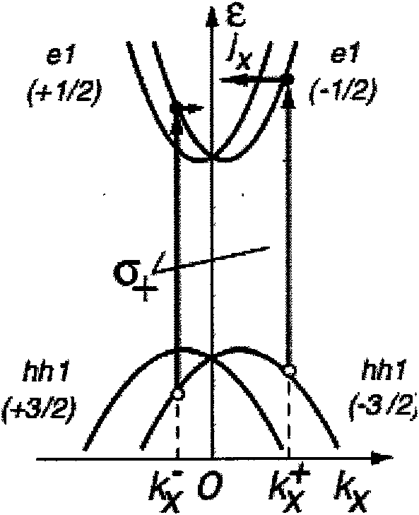
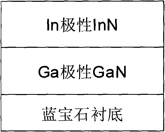
[0019] The invention utilizes the circular photo-galvanic effect (CPGE, circular photo-galvanic effect) to judge the polarity of the semiconductor crystal or the epitaxial thin film. Circularly polarized spin photoelectric effect means that in semiconductor crystals or semiconductor low-dimensional structures lacking spatial inversion symmetry, a weak unbiased directional current will be formed by circularly polarized light irradiation, and the magnitude of the current changes with the helicity of the incident light. The currents generated by left and right circularly polarized light are equivalent and reversed. It is worth emphasizing that only semiconductor materials la...


PUM


Abstract

The invention discloses a method for testing the polarity of semiconductor crystal or epitaxial thin film material, comprising the following steps: irradiating the semiconductor crystal or epitaxial thin film material which is to be tested by utilizing circular polarized light, testing the current direction of the generated no-bias current; and judging the polarity of the semiconductor crystal or epitaxial thin film material which is to be tested according to the current direction of the no-bias current. In addition, the invention further discloses a system for testing the polarity of the semiconductor crystal or epitaxial thin film material. The test system in the invention can work under normal temperature and normal pressure, has high test accuracy, simple and speedy sample preparation, and high test speed, is non-destructive to the tested samples, and has low demand towards the testing personnel with easy operation; the test time of each sample is only 10 minutes; what is more, the whole set of test system is low in price and can greatly reduce test cost.

Description

technical field [0001] The invention relates to the field of semiconductors, in particular to a method and a detection system for detecting the polarity of semiconductor crystals or epitaxial thin film materials. Background technique [0002] In recent decades, optoelectronic devices based on III-V and II-VI compound semiconductor materials have been widely used and created huge economic benefits. As the basis of optoelectronic devices, the growth and physical properties of high-quality III-V and II-VI compound semiconductor materials are particularly important. For the above-mentioned semiconductor materials, the polarity or polarization effect due to the non-centrosymmetric structure has a strong impact on the properties of the semiconductor, especially the optoelectronic properties of its epitaxial film and quantum structure. For example, the polarity of III-nitride wide-bandgap semiconductors has a crucial influence on the optical and electrical properties of the materi...

Claims


Application Information

Patent Timeline
Patent Type & Authority Applications(China)
IPC IPC(8): G01N23/227
Inventor 王新强沈波张琦贺小伟许福军尹春明杨志坚张国义
Owner 东莞燕园半导体科技有限公司
Why Eureka
Try Eureka