Method for manufacturing GaAs-based MHEMT device with grid length of 200nm

A device and gate length technology, applied in the field of compound semiconductor devices, can solve problems such as limiting the application of MHEMT and restricting the performance of MHEMT devices, and achieving the effects of strong reliability, simple and easy process, and strong economical application.

Inactive Publication Date: 2009-12-30
INST OF MICROELECTRONICS CHINESE ACAD OF SCI
View PDF0 Cites 4 Cited by
  • Summary
  • Abstract
  • Description
  • Claims
  • Application Information

AI Technical Summary

Problems solved by technology

The reported MHEMT devices all adopt optical lithography technology, and the gate length is generally about 1.0 μm, which seriously restricts the device performance of MHEMT and limits the application of MHEMT in the high frequency field.

Method used


Image

  • Method for manufacturing GaAs-based MHEMT device with grid length of 200nm
  • Method for manufacturing GaAs-based MHEMT device with grid length of 200nm
  • Method for manufacturing GaAs-based MHEMT device with grid length of 200nm

Examples


Embodiment Construction

[0037] In order to make the object, technical solution and advantages of the present invention clearer, the present invention will be described in further detail below in conjunction with specific embodiments and with reference to the accompanying drawings.

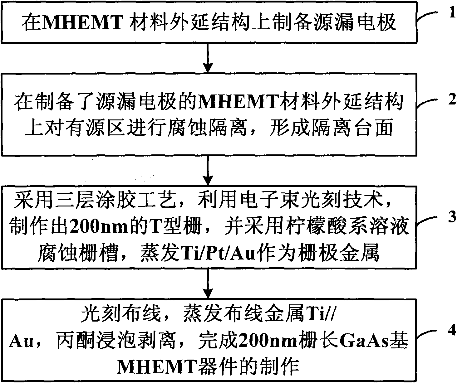
[0038] Such as figure 1 as shown, figure 1 It is a flow chart of a method for making a GaAs-based MHEMT device with a gate length of 200nm provided by the present invention, and the method includes the following steps:

[0039] Step 1: Prepare source and drain electrodes on the epitaxial structure of the MHEMT material; the specific process includes:

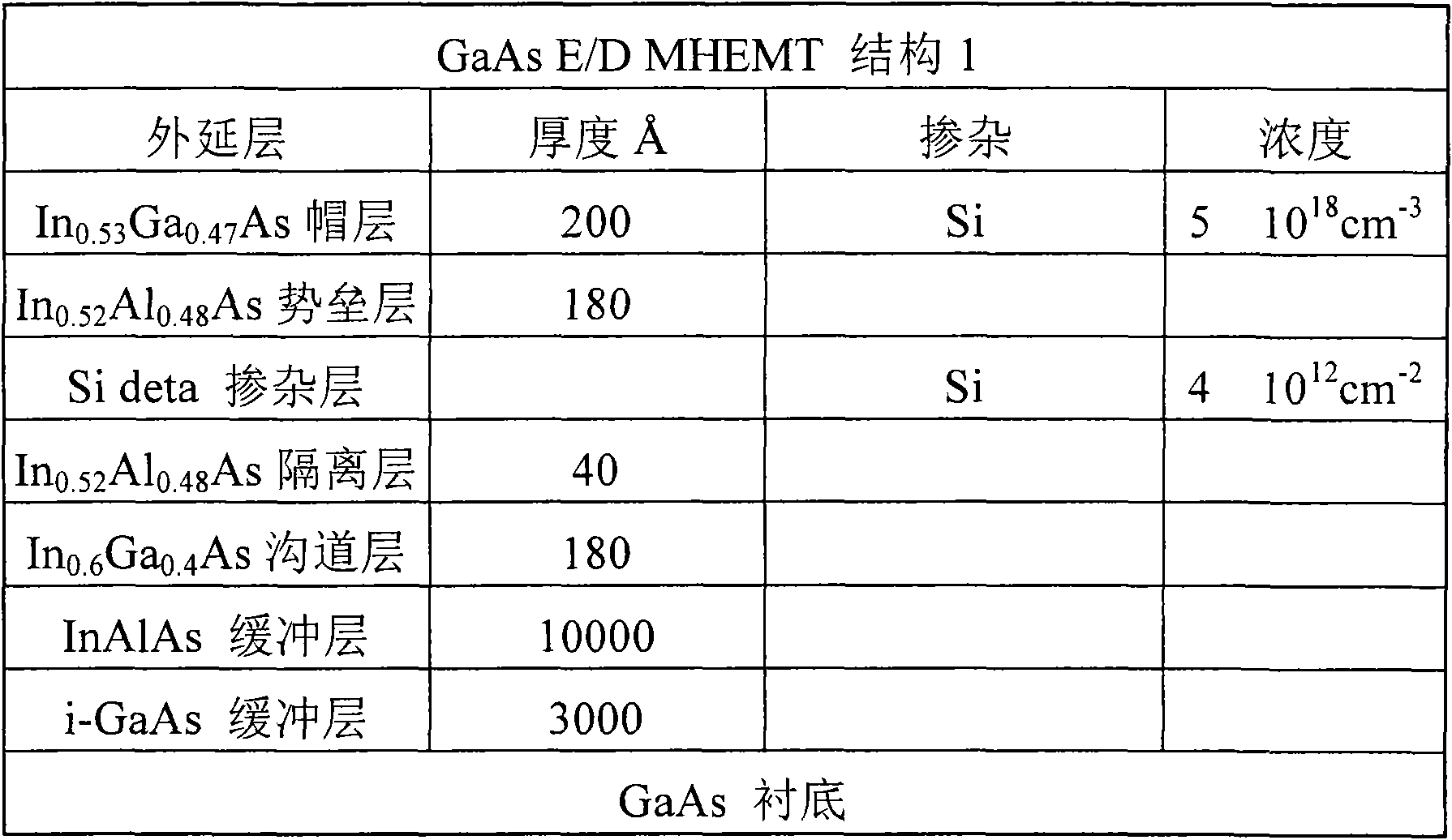
[0040] In the MHEMT material epitaxial structure (such as figure 2 As shown) apply collagen glue AZ5214 on top, 3500 rpm, apply for 1 minute, the coating thickness of the original glue AZ5214 is about 1.6 μm, 95 ℃ hot plate, 90 seconds, source and leak version, small machine exposure for about 20 seconds, AZ5214 Developing solution for about 60s, rinse with water, apply...


PUM

PropertyMeasurementUnit
Thicknessaaaaaaaaaa
Thicknessaaaaaaaaaa
Thicknessaaaaaaaaaa

Abstract

The invention discloses a method for manufacturing a GaAs-based MHEMT device with grid length of 200nm, which comprises the following steps: preparing source and drain electrodes on an epitaxial structure of an MHEMT material; corroding and isolating an active area on the epitaxial structure of the MHEMT material with the prepared source and drain electrodes to form an isolated table top; adopting a thee-layer gluing process and manufacturing a T-shaped grid of 200nm by using electron beam lithography technology, adopting citric acid solution to corrode a grid groove, and evaporating Ti / Pt / Au as grid metal; and photoetching wiring, evaporating the wiring metal Ti / Pt / Au, and carrying out acetone soaking and peeling to finish the manufacture of the GaAs-based MHEMT device with the grid length of 200nm. The method manufactures the GaAs-based MHEMT device with the T-shaped grid structure, obtains superior direct current, high frequency and power performances, and lays a foundation for further researching the high-performance GaAs-based MHEMT device.

Description

technical field [0001] The invention relates to the technical field of compound semiconductor devices, in particular to a method for manufacturing GaAs-based MHEMT devices with a gate length of 200nm by electron beam lithography technology. Background technique [0002] In recent years, the demand for microwave / millimeter wave high-speed data transmission and broadband applications is increasing, such as high-speed optical fiber transmission system (40Gbit / s), microwave point-to-point radio communication system, local multipoint distribution service, Ka-band satellite communication, 77GHz automotive Anti-collision radar and other fields have greatly promoted the progress of the microelectronics industry. [0003] GaAs-based pseudomorphic high electron mobility transistors (pseudomorphic high electron mobility transistor, PHEMT) and InP-based high electron mobility transistors (high electron mobility transistor, HEMT) have been recognized as having great potential in microwav...

Claims


Application Information

Patent Timeline
IPC IPC(8): H01L21/331H01L21/28
Inventor 黎明张海英付晓君徐静波
Owner INST OF MICROELECTRONICS CHINESE ACAD OF SCI
Why Eureka
Try Eureka