Semiconductor device, test mould and test method

A technology for testing molds and semiconductors, which is applied in the field of semiconductors, can solve the problems of increasing the test cost of semiconductor devices, increasing test costs, and large on-state voltage drop, and achieves the goals of reducing test cost, improving thermal resistance performance, and reducing on-state voltage drop Effect

Active Publication Date: 2009-12-30
ZHUZHOU CRRC TIMES SEMICON CO LTD
View PDF0 Cites 6 Cited by
  • Summary
  • Abstract
  • Description
  • Claims
  • Application Information

AI Technical Summary

Problems solved by technology

However, if the test result is unqualified, it will damage both the tested die chip and the rhodium-molybdenum test piece group used for testing. The damage of the tested chip is a natural result of test screening, but the damage of the rhodium-plated molybdenum test piece group increases. reduces the cost of testing such

Method used


Image

  • Semiconductor device, test mould and test method
  • Semiconductor device, test mould and test method
  • Semiconductor device, test mould and test method

Examples


Embodiment Construction

[0031] The technical solutions of the present invention will be described below with reference to the accompanying drawings and embodiments.

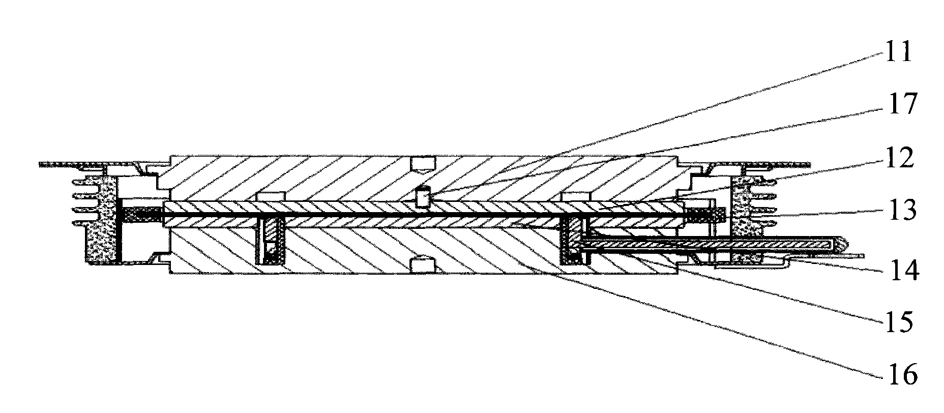
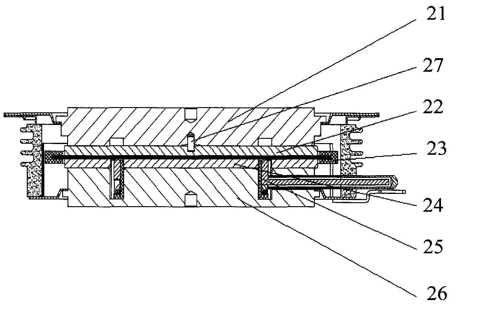
[0032] refer to figure 2 , is a schematic cross-sectional view of the structure of a semiconductor device according to an embodiment of the present invention.

[0033] In the present embodiment, the semiconductor device adopts an aluminum alloy component group instead of a rhodium-plated molybdenum component group as a package component of a fully crimped device. The semiconductor device may include a tube cover 21 , an aluminum alloy anode 22 , a die chip 23 , an aluminum alloy cathode 24 , a gate electrode 25 and a stem 26 which are stacked and connected in sequence. The adjacent components of each layer are electrically connected and the gate electrode is also electrically connected to the die chip 23 . The connection method of each part is the same as that in the prior art.

[0034] The tube cover 21 is used as the anode of the ...


PUM


Abstract

The embodiment of the invention provides a semiconductor device, a test mould and a test method. The semiconductor device comprises a tube cap, an aluminum alloy anode, a tube core chip, an aluminum alloy cathode, a gate pole and a tube socket orderly stacked; and adjacent layers of components are electrically connected, and the gate pole is electrically connected with the tube core chip. The test method for the semiconductor device comprises the following steps: assembling a tube core chip to be tested, the gate pole component and an aluminum alloy test sheet group into a test fixture, wherein the tube core chip to be tested is sandwiched between the anode and the cathode of the aluminum alloy test sheet group; and performing dynamic testing. The method adopts the aluminum alloy sheet group to replace a rhodium plated molybdenum sheet group in the prior art, not only reduces testing cost, but also reduces turn on voltage drop, improves thermal resistance performance, and improves the combination with the surface of the tube core chip.

Description

technical field [0001] The invention relates to the technical field of semiconductors, in particular to a semiconductor device, a test mold, and a test method. Background technique [0002] Fully-controlled power semiconductor devices such as gate turn-off thyristor (GTO) and integrated gate commutated thyristor (IGCT) have the characteristics of silicon rectifier devices, and can work under high voltage and high current conditions, and their switching process can be controlled by Gate control, so it is widely used in power electronic circuits such as controllable rectification, AC voltage regulation, contactless electronic switches, inverters and frequency conversion. [0003] The packaged structure of such fully controlled power semiconductor devices, such as figure 1 As shown, it generally includes a tube cover 11, a metal sheet group as the anode 12, a tube core 13, a metal sheet group as the cathode 14, a gate electrode 15 and a tube base 16, and may also include a tub...

Claims


Application Information

Patent Timeline
IPC IPC(8): H01L23/48H01L21/66G01R31/26
Inventor 张明李继鲁蒋谊彭文华刘旭君
Owner ZHUZHOU CRRC TIMES SEMICON CO LTD
Why Eureka
Try Eureka